 Facebook
 Google
 GitHub
 Linkedin
Understanding the Operation of a Boost Converter
Learn how a step-up switching regulator generates an output voltage higher than its input voltage.
In my previous article, we examined the basic topology of a boost converter (Figure 1).
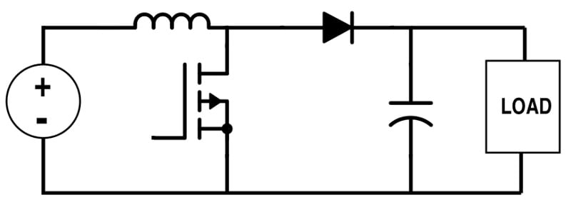
Figure 1. Generic topology for a boost converter.
We then worked through a design procedure in which we configured the power stage of a simulated boost converter for use in a mixed-signal, battery-powered device. Figure 2 shows the application-specific LTspice implementation we created.
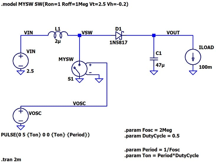
Figure 2. Schematic of a boost converter implemented in LTspice.
In this article, we’ll use the same circuit to explore the electrical behavior that makes step-up conversion possible.
The Switch-On State
As with the buck converter, the boost converter has two fundamental operational states: one when the power switch is closed (the switch-on state), and one when it is open (the switch-off state). Let’s start with the switch-on state.
When the switch is conducting, current from the input supply is shunted to ground. It flows through the inductor, through the switch, and into the ground node, as seen in Figure 3. It doesn’t pass through the diode or reach the capacitor. During this time, the inductor’s current is ramping up and the inductor is “charging,” by which I mean that the energy content of its magnetic field is increasing.
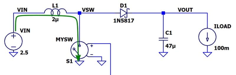
Figure 3. The path of supply current through a boost converter in the switch-on state.
Meanwhile, the load circuitry needs a consistent supply of current: to make the diagram more complete, we need to include the load current (Figure 4). As you can see, the capacitor discharges and provides load current during the switch-on state.
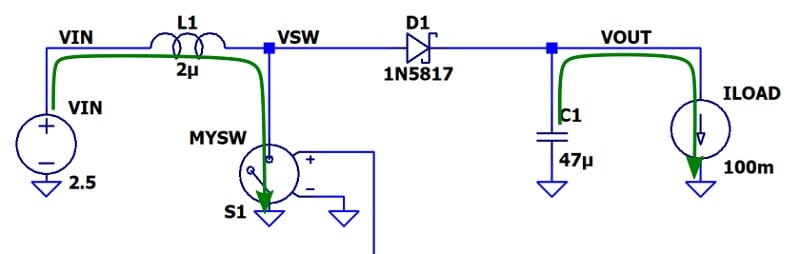
Figure 4. A boost converter in the switch-on state. Supply current and load current are both indicated in green.
The inductor is charging, the capacitor is discharging, and the diode blocks current in both directions because it is reverse-biased.
But how do we know that the diode is reverse-biased? The key observation is that the impedance of the closed switch is very low: the voltage at the VSW node will therefore be close to 0 V. Since the output voltage is above 0 V, the diode is reversed-biased and no current flows as long as the switch is conducting.
Recognizing that the diode is an open circuit during this portion of the switch cycle underlines the importance of the output capacitor, which is the only component available for maintaining output voltage and delivering load current when the switch is on. It’s also worth noting that the diode prevents the output voltage from driving current back to ground through the closed switch.
The Switch-Off State
Current was flowing through the inductor when the switch was closed, and we know that it is the nature of inductance to resist changes in current flow. Therefore, inductor current will continue to flow when the switch opens, taking the only reasonable pathway available: the diode.
In the process of forcing its current through the diode, the inductor must raise the voltage at node VSW until the diode is forward-biased. For this to occur, the inductor must generate a VSW voltage that is equal to at least (VOUT + VF), where VF denotes the forward voltage of the diode. The voltage at the right-hand terminal of the inductor will thus be greater than VOUT as well as greater than VIN.
Once the voltage across the diode is sufficient for conduction, current will flow from the source, through the inductor and diode, and into the capacitor and load (Figure 5).
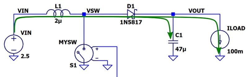
Figure 5. Current flow through a boost converter in the switch-off state.
Achieving Boost
Capacitors can charge up to voltages that exceed the supply voltages in a system. This is evident from the equation that relates the capacitance (C), stored charge (Q), and voltage (V) of a capacitor:
$$V=\frac{Q}{C}$$
If you drive more charge onto the plates of a capacitor, voltage increases. There’s nothing in this equation to suggest that the voltage will level off when you approach the system’s supply voltage.
However, we also have other electrical laws to consider, and usually the capacitor’s voltage doesn’t increase beyond the supply voltage. A capacitor’s voltage naturally levels off at the voltage used to drive charge onto its plates.
To successfully increase capacitor voltage beyond the driving voltage, we need to “pump” charge into the capacitor and prevent charge from flowing back into the source. The boost converter’s diode, which functions as a one-way valve for current, provides both of these actions:
- Inductor current can flow through the diode and charge up the capacitor to voltages above VIN.
- The capacitor cannot discharge back into the source via the inductor because the diode prevents current flow in that direction.
Figure 6 shows the flow of current from the inductor in green and from the capacitor in red.
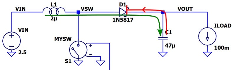
Figure 6. The diode permits current to flow from the inductor to the capacitor, but not vice versa.
In short, a boost converter stores energy in an inductor’s magnetic field, then transfers that energy to a capacitor in such a way that the capacitor’s voltage can increase beyond the voltage of the source that supplied energy to the inductor.
What’s Next
I hope that this article has helped you gain an understanding of how the components in a boost converter work together to generate a regulated output voltage that is higher than its input voltage. In the next article, we’ll use simulated voltage and current waveforms to investigate this circuit more thoroughly.
All images used courtesy of Robert Keim


Very good explanation. Thanks
The next would be a alternating stage Boost converter. With this you can understand how this works: https://youtu.be/3ISDvOFCF44?feature=shared
Very very very good explanation. Wo!