Facebook
 Google
 GitHub
 Linkedin
High Efficiencies at Light Loads: A Voltage Boost Converter from Texas Instruments
Texas Instruments recently released their new voltage boost converter (step-up converter) that offers high efficiencies at light load conditions.
Texas Instruments recently released their new voltage boost converter (step-up converter) that offers high efficiencies at light load conditions.
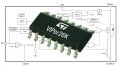
Texas Instruments' TPS61322xx is a boost, or step-up, voltage converter with a low quiescent current of 6.5 µA. According to the datasheet (PDF), this boost converter is based on a hysteretic current-mode control topology using synchronous rectification; this configuration allows for high efficiencies under light-load conditions. If you didn't know, a voltage regulator that employs a hysteretic architecture can also be known as a ripple regulator—according to this Texas Instruments app note (PDF-page 3)—or a bang-bang regulator—per this Microsemi technical note (page 13).
As it's explained in the TI app note above, the fundamental difference between a non-hysteretic architecture (known as a PWM architecture) and a hysteretic-type design is how the converter's "switching action is generated once the desired inductor current (Vc) is known."
A falling-edge PWM design switches on at regularly spaced time intervals and switches off once a specified threshold voltage has been reached. The result is a constant frequency ripple voltage with varying ripple amplitude.
The hysteretic architecture has variable frequency timing, meaning it switches on when a low voltage threshold is passed and off when a high voltage threshold is passed. The result is a varying frequency ripple voltage with constant ripple amplitude.
The hysteretic technique maintains "the current ripple amplitude," hence the name ripple regulator. Section 8.3.2 (entitled Boost Controller Circuit) on page 8 of the TPS61322xx datasheet explains that the IC regulates its output voltage by keeping the inductor ripple current at a constant 200 mA. As can be seen in the figure below, this 200 mA fixed ripple current is maintained when the converter enters the discontinuous current mode, or DCM. It is this discontinuous current mode that allows the device to achieve high efficiencies under light load conditions.

200 mA of inductor ripple current is maintained during continuous and discontinuous modes of operation. Plot taken from the datasheet (PDF).
Output Voltage: Set by the Part Number
As described in the section entitled Description on page 1 of the datasheet, the output voltage of this boost converter is set internally to a fixed level ranging from 1.8V to 5.5V, in increments of 100mV. However, according to the website, these ICs are still in the pre-production stages. If you want to integrate one of these into a new design, submit a sample request with TI.

The IC's part number determines the voltage output setting. Currently, only a limited number of output voltages are available. Table courtesy of the datasheet (PDF).
High Efficiencies...at Light Loads
While this IC is indeed capable of delivering high efficiencies during light-load conditions, the IC's efficiency performance significantly decreases with larger loads, as is illustrated in the following figure. Since the graph in the figure below references part number TPS61322, it can be assumed that these curves are only valid for an output voltage of 2.2V (per the information contained in the table above). The efficiency curves are listed in input voltages of 0.3V increments. As you can see, the load efficiency while using a 4.7 µH inductor drops off significantly as the output current exceeds 0.1A, which is much less than the current limit of the IC of 0.75A.

The efficiency of this IC drops significantly at high-load conditions. Plot taken from the datasheet (PDF).
Unfortunately, the figure above displays the only Load Efficiency with Different Inputs graph in the datasheet. And while page 13 offers an Efficiency with Different Inductance graph (see figure below), it would be very helpful if additional efficiency curves were made available. Additional information can be obtained using TI’s Webench design simulator.

While this efficiency graph is indeed helpful, more like it with varying values of VIN, VOUT, and IOUT would be very useful. Taken from the datasheet (PDF).
Applications and Examples
If you're interested in reviewing a few typical application circuits, then check out the Application and Implementation section on page 9 of the datasheet. Within this section, TI focuses on two applications circuits: one without the use of an optional Schottky diode, and one with the Schottky diode. These two application examples include schematics (see figure below), equations, design parameters, and even recommended inductors and capacitors along with their manufacturers and associated part numbers.

The datasheet includes application example information, such as these two circuits. Note that only the bottom circuit employs the external (optional) Schottky diode.
Have you had a chance to use this new boost voltage converter from TI, the TPS61322xx? If so, leave a comment and tell us about your experiences.