Facebook
 Google
 GitHub
 Linkedin
Converter Evaluation and Design
List of common converters and calculations of switch stresses/utilization are presented in this article. Converter design with the aid of computer spreadsheet is also shown here. A short list of converters is provided based on the basic topologies and circuit manipulations of the converters discussed on other technical articles.
Switch Stresses in Basic Converters and Other Important Converter Parameters/Design
Recommended Level
Intermediate
A Short List of Converters
There are innumerable types of converters possible. A short list of converters is provided based on the basic topologies and circuit manipulations of the converters discussed in other technical articles.
Watkins-Johnson converter, Inverse Watkins converter, Current-fed Bridge converter and Bridge converter can be obtained when the inductor terminals are connected to single-pole double-throw (SPDT) switches in different ways. These are also called H-Bridge converters.
- Buck Converter
- Boost Converter
- Inverting Buck-Boost Converter
- Non-Inverting Buck-Boost Converter
- Cuk Converter
- Bridge Converter
- Watkins-Johnson Converter
- Inverse Watkins Johnson Converter
- Current-Fed Bridge Converter
- SEPIC Converter
- Inverse SEPIC Converter
- Transformer Isolated Converters
Switch Stress and Utilization
Switching losses are usually more dominant than any other losses in the converter. Thus, maximum value of voltage VM and current IM applied to the switches must be minimized keeping the load power maximum.
Stress for the n switches in the converter is defined as,
Stress,
$$S=\sum_{i=0}^{n}(V_{Mi} \,x \,I_{Mi})$$
Sometimes R.M.S value of the current across the switch is also taken,
$$S=\sum_{i=0}^{n}(V_{Mi}\, x \,I_{Ri})$$
If the stresses in the switches of the converter are less, there will also be lesser amount of silicon required. Moreover, current gain, switching speed and storage time are also dependent on the stresses across the switch.
If the load power for the circuit is P, then switch utilization for a converter is defined as $$U=\frac{P_{O}}{S};$$ i.e. output power obtained per unit of switch stress. This is the scale to know how the converter utilizes its devices.
Now, consider the non-isolated buck converter as shown in Fig.1.
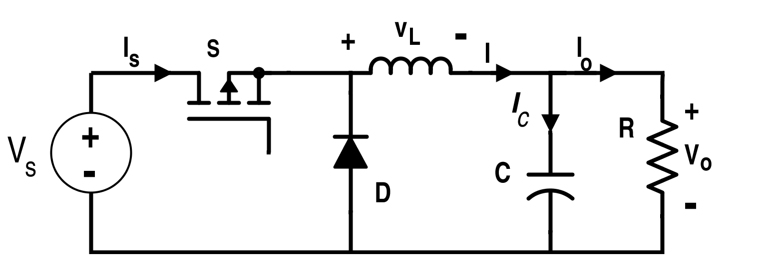
Figure 1. Circuit for Buck Converter
For the buck converter, conversion ratio is $$\frac{V_{O}}{V_{S}}=D.$$
where D is the duty ratio for the switch S
The maximum value of stress applied across the switch is ,
$$S=V_{m} I_{m}=V_{S}(1+r_{C})I_{O}(1+r_{L})$$
In the buck converter, input voltage is more than the output voltage and the output current is more than the input current for the same input and output power. Also note that the direction of current is unidirectional i.e. from input to output.
Here, rc is the ripple ratio for the voltage across the capacitor and rL is the ripple ratio for the current across the inductor:
$$r_{C}=\frac{\frac{ΔV_{S}}{2}}{Vs}$$ and $$r_{L}=\frac{\frac{ΔI_{L}}{2}}{I_{L}}.$$
Thus,
$$S=V_{S}(1+r_{C})I_{O}(1+r_{L})=\frac{V_{O}I_{O}}{D}(1+r_{C})(1+r_{L})=\frac{P_{O}(1+r_{C})(1+r_{L})}{D}$$
Stress (S) will be minimum when D=1; i.e. when the conversion ratio of the buck converter is in unity, stress will be minimum across the switch.
Maximum value of voltage across the switch for the buck converter is equal to $$V_{S}.$$
R.M.S current through the switch S for the buck converter is equal to $$\frac{I_{S}}{\sqrt{D}}.$$
If the R.M.S value of current is considered for the stress calculation, stress for the switch S is,
$$S=V_{S}\frac{I_{S}}{\sqrt{D}}=\frac{P_{O}}{\sqrt{D}}$$
The switch utilization ratio for the non-isolated buck converter is,
$$U=\sqrt{D}$$
Similarly, stress for non-isolated boost converter will be minimum when the conversion ratio is in unity.
.png)
Figure 2. Circuit for Boost Converter
Maximum value of the voltage across the switch for the boost converter is,
$$V_{O} =\frac{1}{1-D}V_{S}$$
R.M.S current across the switch in the case of the boost converter is equal to $$I_{S}\sqrt{D}.$$
The stress for the switch S is, $$S = V_{S}\frac{I_{S}\sqrt{D}}{(1-D)}=\frac{P_{O}(\sqrt{D})}{(1-D)}$$
The switch utilization ratio for the boost converter is, $$U =\frac{1-D}{\sqrt{D}}$$
Note that the maximum value of utilization factor for buck converter is in unity which occurs at D=1; while the maximum value of utilization factor for boost converter is in infinity which occurs at D=0.
Now, consider the buck-boost converter shown in Fig. 3.
.png)
Figure 3. Circuit for Buck-Boost Converter
In the case of buck-boost converter, maximum voltage and maximum current across the switch S is the sum of their respective input and output parameters as they are of opposite polarity.
The stress across the switch S is given by
$$S=V_{m}I_{m}=(\left|V_{S}\right|+\left|V_{O}\right|)(1+r_{C})(\left|I_{S}\right|+\left|I_{O}\right|)(1+r_{L})$$
$$\Rightarrow S\,=\,\frac{P_{o}(1+r_{C})(1+r_{L})}{D(1-D)}$$ which will be minimum when D=0.5.
The stress is minimum when the conversion ratio is in unity:
$$\frac{V_{O}}{V_{s}}=\frac{D}{1-D}.$$
Maximum voltage across the switch is,
$$V_{M}=V_{S}+V_{O}=V_{S}+\frac{D}{1-D}V_{S}=\frac{1}{1-D}V_{S}.$$
R.M.S. value of current across the switch is equal to
$$\frac{I_{S}}{\sqrt{D}}.$$
If the R.M.S. value of current is considered for the switch for the stress calculation,
Stress for the switch
S $$= \frac{V_{S}I_{S}}{(1-D)\sqrt{D}}=\frac{P_{O}}{(1-D)\sqrt{D}}$$
Utilization factor for the buck-boost converter is equal to
$$(1-D)\sqrt{D}.$$
Similarly, Cuk converter has the minimum stress as its conversion ratio is in unity. As the voltages and currents are added up in the Cuk or buck-boost converter, the stress across the switch in these cases is larger compared to the stress in the boost or buck converter switches.
Fig.4 shows the graph for the stress w.r.t. the conversion ratio for the mentioned converters above.
.png)
Figure 4. Switch Stress vs Conversion Ratio Graph
Hence, it is not wise to use buck-boost or Cuk converter unless we require the negative output voltage or the features offered by the buck and boost from the same converter due to high stress in the converter during high-power applications.
Consider the flyback converter as shown in Fig. 5.
.png)
Figure 5. Circuit for Flyback Converter
The maximum voltage across the switch S is,
$$V_{S}+\frac{N1}{N2}V_{O}.$$
R.M.S current across the switch S is,
$$I_{S}\sqrt{D}=\frac{P_{O}}{(V_{S}\sqrt{D})}$$
The stress across the switch S is,
$$(V_{S}+\frac{N1}{N2}V_{O})(I_{S}\sqrt{D})$$
Also,
$$P_{O}=(1-D)(V_{O} I_{O})(\frac{N1}{N2}).$$
Conversion ratio for the flyback converter is,
$$\frac{V_{O}}{V_{S}}=\frac{N2}{N1}\frac{D}{1-D}$$
The switch utilization factor for the flyback converter is,
$$U = (1-D)\sqrt{D}.$$
Design with the Help of Computer Spreadsheet
The spreadsheet provided by the manufacturer acts as a tool for getting the converter design parameters with necessary trade-off for the stresses using the fundamental equations of that converter. Spreadsheet specifies the maximum and minimum values of currents and voltages, turns ratio for the transformer isolated converter, current and voltage ripple, maximum and minimum values of duty cycle, worst-case stresses and switches utilization, switching frequency and etc. Here, the computer spreadsheet can act as an efficient way to determine how these factors affect the element voltage and current stresses.
The typical example of the spreadsheet provided by MAXIM is given in Table 1.
.png.png)
Table 1. Spreadsheet for the Boost Converter by MAXIM
The necessary formulas for the boost converter in continuous and discontinuous conduction mode are given below.
.png.png)
Table 2. Equations for the Boost Converter in Continuous and Discontinuous Conduction Mode
You can go to the following URL link to get the spreadsheet for buck and boost converters by ON Semiconductor.
www.onsemi.com/pub/Collateral/NCP3066%20DESIGN%20TOOL.XLS