Facebook
 Google
 GitHub
 Linkedin
Introduction to the Boost Converter: Structure and Design
What is a boost converter? This article discusses key initial design tasks for a step-up voltage regulator and describes its structure.
In my last article series, LTspice helped us to examine the features of a step-down switching regulator’s power stage. The next batch of articles will continue using LTspice to explore the design and electrical behavior of switch-mode power supplies, but with a focus on regulator topologies other than the buck converter.
We’ll start off with the circuit commonly known as a boost converter or step-up regulator. In this article, we’ll discuss its design; in future articles, we’ll explore its basic operation and take a close look at current and voltage waveforms.
The Boost Converter Power Stage
As the names ‘boost’ and ‘step-up’ both imply, the topology we’re discussing today can achieve an output voltage higher than its input voltage. This—along with improved efficiency—represents a crucial advantage of switch-mode over linear regulation, since the latter cannot produce VOUT higher than VIN.
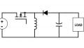
With switch-mode techniques, however, all we need is a different arrangement of the same simple components that we used for the step-down converter. Figure 1 shows what this step-up arrangement looks like.

Figure 1. Circuit diagram of a step-up voltage regulator. Image used courtesy of Robert Keim
Now I’ll create a boost converter design for LTspice. As with the LTspice buck converter, I’ll use a voltage-controlled switch instead of a transistor.
My implementation is below, in Figure 2: it represents a circuit intended for low-voltage, battery-powered applications, and the values I’ve chosen reflect this. I’ll go into more detail on that in the coming section.

Figure 2. Schematic of a boost converter implemented in LTspice. Image used courtesy of Robert Keim
Is it a boost regulator or a boost converter? Check out What is a Switching Voltage Regulator? for a review of terminology and basic concepts.
Operating Parameters and Component Values
Before running simulations based on this schematic, let’s consider our boost converter’s parameters.
Input and Output Voltage
The boost converter’s 2.5 V source provides an input voltage we might get from a pair of partially discharged alkaline coin-cell batteries. As with other switchers, though, the completed circuit—i.e., the power stage combined with a feedback system for output voltage regulation—will be compatible with a range of input voltages. The same circuit could therefore be combined with a 3 V lithium-ion coin cell or a single alkaline cell.
The specified output voltage is 5 V. I can imagine a device in which this 5 V directly supplies some higher-power drive circuitry and a connected sensor or relay module, with the 5 V subsequently passing through one or more compact linear regulators for lower-power digital circuitry and high-precision analog circuitry. I like this sort of power-management solution: despite the gradually diminishing battery voltage, it gives us a stable 5 V rail that reliably supplies power, either directly or indirectly, to all the components in the system.
Duty Cycle
The idealized relationship between input voltage, output voltage, and duty cycle for a boost regulator is as follows:
$$D=1-{\frac {(V_{IN}\times\text{efficiency})}{V_{OUT}}}$$
We have VIN = 2.5 V and VOUT = 5 V. Since I’m not going to deliberately incorporate non-idealities into my simulation, I’ll leave the efficiency at 100%. This gives us a duty cycle of 50%.
For those who haven’t read the preceding articles, I want to emphasize that we can’t rely on a fixed duty cycle to produce the desired output voltage. The equation above gives us a starting point, but in a real implementation we would rely on closed-loop control to adjust the duty cycle as needed to maintain the proper VOUT.
Inductance
I determined the original inductance value for my LTspice buck converter by using a formula. When I tried using the same approach for the boost converter, however, my first attempt produced an inductance value about an order of magnitude larger than what I would prefer to use in a compact, low-voltage device.
Fortunately, this calculated inductance isn’t necessary for successful converter operation: instead of looking for a different formula, I just chose a value that conformed to my proposed size constraints and used that instead. The 2 μH inductance shown in Figure 2 is based on the boost converter inductance recommendations in this Texas Instruments application note, which also contains the formula I initially used and other useful information on inductor selection.
Switching Frequency
Because I chose a rather small inductance, I also chose a higher switching frequency. This is one of the fundamental relationships in switching-regulator design: higher switching frequency allows for lower inductance. I have fOSC at 2 MHz, which is rather high for a switcher but not at all unrealistic.
Output Capacitance
You can use the following formula to calculate a satisfactory output capacitance based on expected output current (IOUT), duty cycle (D), switching frequency (fOSC), and desired output ripple (ΔVOUT):
$$C_{OUT}=\frac{I_{OUT}\times D}{f_{OSC}\times\Delta V_{OUT}}$$
Based on the application characteristics I described above, though, there’s no particular need to keep ripple low. The circuit can also—as I suggested earlier in the article— be connected to a linear regulator, in which case it will get the benefit of the linear regulator’s ripple-suppression capability.
I ultimately decided to skip the calculations. As with the inductance, I used recommendations for real-life integrated circuits to arrive at a value that I considered a good compromise between performance and size.
Linear Regulator PSRR
While we’re on the topic, a linear regulator’s ripple-suppression capability is measured as PSRR (power supply rejection ratio). PSRR fluctuates based on several parameters, including frequency; the plot below (Figure 3) shows such a fluctuation.

Figure 3. A graph of PSRR relative to ripple frequency. Image used courtesy of Texas Instruments
Though we still have plenty of attenuation at 2 MHz, this plot provides an argument in favor of selecting a lower switching frequency if you plan to use a linear regulator to reduce output ripple amplitude.
Diode Reverse Recovery Time
We have one more parameter to discuss: the reverse recovery time of the converter’s diode, which is particularly important to switching regulators (if you’re interested in learning more, this article on choosing the right rectifier for your power circuitry is a great resource).
Though I used a standard diode for the buck converter, I chose a Schottky diode for the boost converter. Schottky diodes are generally preferred for switching regulators because they more efficiently switch between the conducting and non-conducting states and have a lower voltage drop when conducting.
What’s Next
We’ve gone through quite a bit of information pertaining to the initial design tasks for the power stage of a step-up switching regulator. In the next article, we’ll begin discussing the regulator’s actual operation—so if you’re still a bit perplexed as to how this circuit actually generates an output voltage higher than the input voltage, stay tuned!
Related Content