Facebook
 Google
 GitHub
 Linkedin
All About the Inverting Buck-Boost Converter
Learn about the inverting buck-boost converter, a switching voltage regulator designed to handle unstable input voltages.
Inductor-based, switch-mode voltage conversion is an essential technique for circuit designers. It allows us to achieve step-down and step-up regulation with circuits that are highly efficient and compact, without introducing excessive complexity in the process.
I covered step-down and step-up regulators in previous articles, and today we’ll learn about another of the fundamental switching regulator topologies: the inverting buck-boost converter.
When I use the term fundamental in this context, I am referring to circuits consisting of output capacitance along with one inductor, one switch, and one diode. I mention this now to explain why this article covers only the inverting buck-boost architecture, and not the four-switch buck-boost as well.
The basic layout of an inverting buck-boost converter can be seen below, in Figure 1. This circuit accepts a positive input voltage and produces a negative output voltage, which can be either larger or smaller than the input voltage.
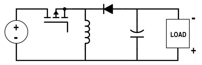
Figure 1. Generic topology of an inverting buck-boost converter.
Now it’s time for me to create an implementation in LTspice.
Want to review the fundamentals before diving in? Read “What is a Switching Voltage Regulator?” for a review of general concepts relating to DC-DC converters.
LTspice Circuit Design
While I won’t walk you step-by-step through the schematic design process this time, there are a few aspects I’d like to briefly comment on.
For my buck converter schematic, I adopted a formal approach in which component values were determined with the aid of formulas and performance specifications. For the boost converter, I worked more from example circuits and prioritized the practical objective of maintaining reasonable inductor size.
For this buck-boost converter, though, I relied on intuition supplemented by trial and error. There are several ways to approach the design of switch-mode power supply (SMPS) power stages. Formulas and datasheet recommendations are a great place to start, but don’t be afraid to experiment.
Do make sure to double-check your work. At first, LTspice wasn’t able to successfully run simulations for this circuit, and I eventually realized that I had the current source pointing in the wrong direction! Remember that the VOUT of an inverting buck-boost is negative, and therefore load current flows upward from the ground node.
The final version of my buck-boost schematic can be seen in Figure 2. We’ll use it first to examine the basic operation of an inverting buck-boost converter, then to simulate one for a more detailed analysis.
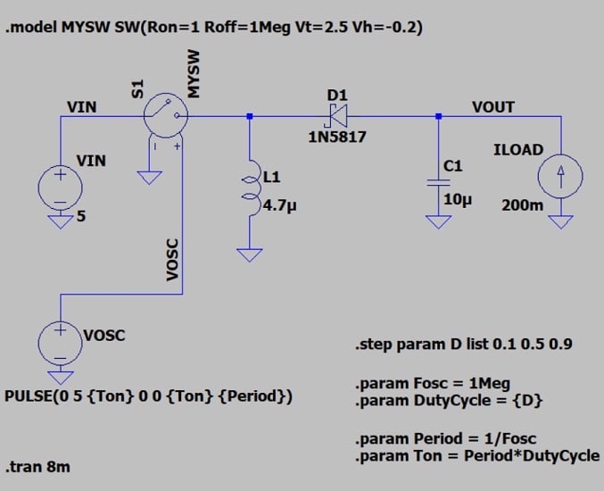
Figure 2. An inverting buck-boost converter implemented in LTspice.
Basic Operation of an Inverting Buck-Boost Converter
As with previous converter topologies, we’ll analyze the buck-boost converter during two distinct operational phases: when the switch is conducting current (the switch-on state), and when the switch is blocking current (the switch-off state). We’ll begin with the switch-on state.
The Switch-On State
Figure 3 shows the path of current through the circuit during the switch-on state: When the switch is conducting, current flows from the input supply, through the inductor, and then to ground.
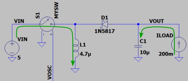
Figure 3. Current flow through a buck-boost converter in switch-on state.
The inductor is charging—its current is ramping up. Meanwhile, the load current is supplied entirely by the output capacitor, which we’re assuming is already charged to the output voltage. It flows upward because VOUT is negative and therefore lower than the ground potential. We’ll see why the output capacitor charges to a negative voltage when we discuss the switch-off state.
Since VOUT is negative and the voltage at the upper terminal of the inductor is approximately equal to VIN, the diode is reverse-biased. However, because of the voltage polarities involved, current would naturally flow from the input side to the output side. The diode’s orientation prevents that.
The Switch-Off State
Figure 4 shows the path taken by current during the switch-off state.
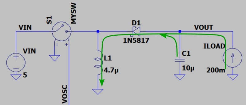
Figure 4. Current flow through a buck-boost converter in switch-off state.
When the switch opens, the inductor attempts to maintain consistent current flow. This causes the voltage at its upper terminal to decrease until the diode is forward-biased. Once the diode is conducting, the inductor functions as an energy source for load current; it also draws current through the capacitor in such a way that the voltage at the capacitor’s upper terminal must be lower than ground. The capacitor charges to a negative voltage, and VOUT becomes negative.
Duty Cycle and Output Voltage
The descriptions of electrical behavior during the switch-on and switch-off states are valid whether the absolute value of the output voltage is higher or lower than the input voltage. The absolute value of VOUT can be controlled via the duty cycle of the oscillator signal: this is how the inverting buck-boost generates a negative voltage that can be larger or smaller in magnitude than the input voltage.
I’ll use the .step statement in Figure 2 to demonstrate this circuit’s ability to generate VOUT magnitudes that are higher than, lower than, or equal to the input voltage. The output voltage is determined by the oscillator’s duty cycle (D).
The idealized relationship is as follows:
$$V_{OUT}=-\left (\frac{D}{1-D}\right )V_{IN}$$
The D values included in the .step statement are:
- 10%, which corresponds to theoretical VOUT of –0.56 V.
- 50%, which corresponds to theoretical VOUT of –5 V.
- And 90%, which corresponds to theoretical VOUT of –45 V.
Now let’s try an LTspice simulation (Figure 5).
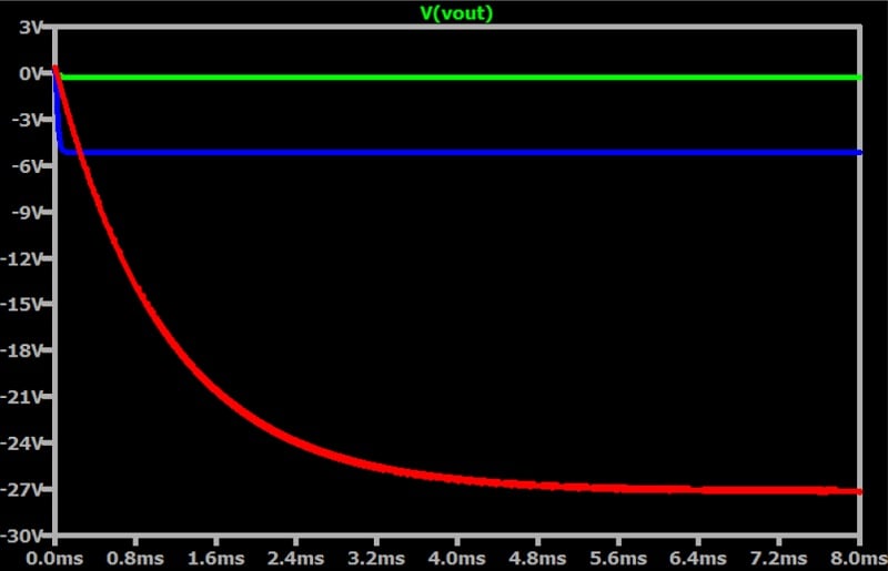
Figure 5. Buck-boost converter output voltage for three different duty cycles.
The simulated output voltages are –0.27 V, –5.2 V, and –27 V. Though these values are vaguely consistent with the theoretical results given above, the differences aren’t trivial. In this instance, the discrepancy between theory and SPICE doesn’t concern me: I’ve seen it before, and I know that the only reliable solution is closed-loop control. We’ll address this issue in more depth in a future article.
Inductor Current and Voltage
Figure 6 shows the relationship between inductor current and switch state.
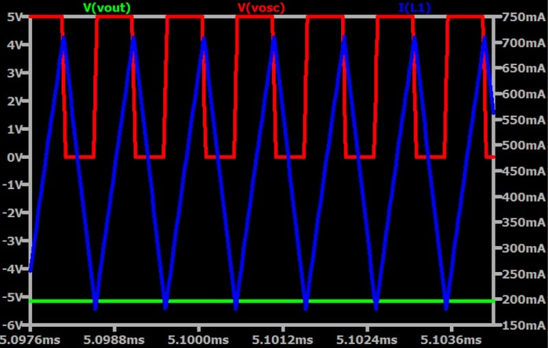
Figure 6. Output voltage, switching voltage, and inductor current for a buck-boost converter.
When the switch closes, inductor current begins to increase, and the inductor stores energy in its magnetic field. When the switch opens, the inductor’s current ramps down as its energy is transferred to the output section of the circuit.
Figure 7 replaces the oscillator signal with the voltage across the inductor. Because it’s also the voltage at the diode’s cathode terminal, the inductor voltage is labeled as VCATHODE.
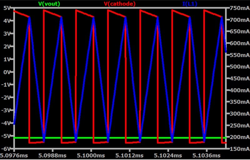
Figure 7. Output voltage, inductor voltage, and inductor current for a buck-boost converter.
When the switch is on, the input voltage and the voltage across the inductor are similar. When the switch turns off, however, the inductor must bring VCATHODE low enough to forward-bias the diode. As you can see in the plot above, VCATHODE decreases to –5.5 V, which is about a diode drop below the –5.16 V output.
Remember that we’re using a Schottky diode, meaning that the diode-drop voltage is significantly lower than the 0.6 or 0.7 V that we get with a typical silicon diode.
Variable Input Voltage
Buck-boost converters are most useful when a specified output voltage must be maintained despite variable input voltage. A battery-powered device, for example, will see a gradually diminishing input voltage as the battery discharges.
I’ve modified the schematic in Figure 2 to produce Figure 8, which we’ll use to demonstrate how appropriate changes in duty cycle can compensate for changes in VIN.
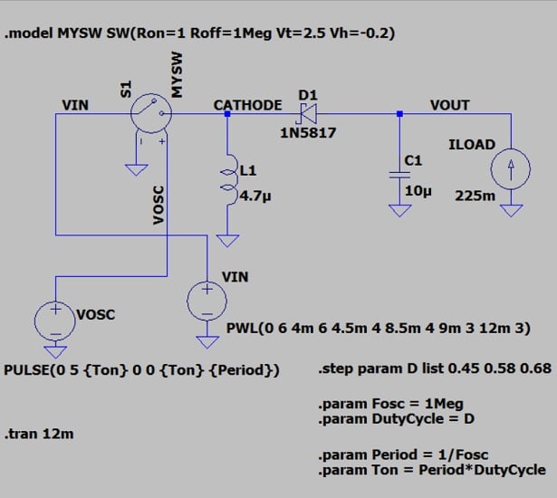
Figure 8. The circuit from Figure 2, but with a modified VIN source and .step statement.
I changed the VIN source from a constant 5 V to a piecewise linear (PWL) function that starts at 6 V, then decreases to 4 V, then decreases again to 3 V. You can see the resulting waveform in Figure 9.
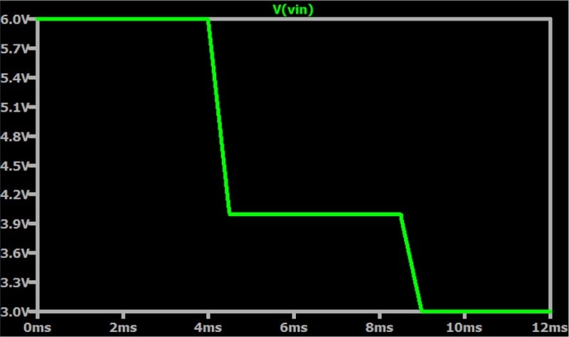
Figure 9. VIN for the buck-boost converter in Figure 8.
I also modified the values in the .step statement to the three duty cycles that are needed to convert 6 V, 4 V, and 3 V into –5 V. These duty cycles are 45%, 58%, and 68%, respectively. I found these values by starting with the VOUT/VIN relationship shown above and then adjusting them via trial and error.
If you run this simulation and plot VIN and VOUT in separate panes, you get Figure 10.
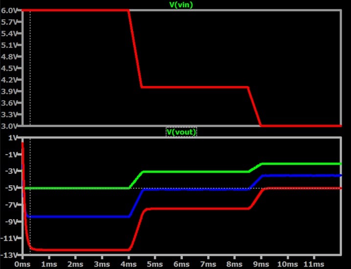
Figure 10. Top pane: VIN. Bottom pane: VOUT for each of the three VIN values above.
Each one of the three VIN levels in the top pane is represented by a different-colored trace in the bottom (VOUT) pane.
To make sense of the VOUT plot, let’s consider each trace over time—in particular, the time during which it intersects the dotted cursor line representing our desired output voltage.
- Green trace: 45% duty cycle. VOUT = –5 V between the 0 ms and 4 ms mark.
- Blue trace: 58% duty cycle. VOUT = –5 V roughly from the 5 ms to 9 ms mark.
- Red trace: 68% duty cycle. VOUT = –5 V from the 9 ms mark to the end of the plot.
We move from green to blue to red—in other words, from 45% to 58% to 68% duty cycle.
The Inversion Problem
We already know that this topology accepts a positive input voltage and produces a negative output voltage. If the load circuitry doesn’t need to share a reference potential with the supply, the output can be treated as positive: ground becomes the supply rail, and the negative VOUT becomes ground. This works for driving current through a high-power LED, for example.
In many applications, though, this won’t be feasible, because the load circuitry cannot function independently of other portions of the system in which signals are referenced to the original ground node. If you’re looking for positive-VIN-to-positive-VOUT regulation, as is often the case, this inversion is a major limitation. That’s why the four-switch topology is a popular alternative: although it requires more components, it has the advantage of producing a positive output voltage.
Wrapping Up
We examined the basics of an inverting buck-boost converter, analyzed some current and voltage waveforms, and created a simplified demonstration of the circuit’s ability to compensate for a battery voltage that begins above the desired output voltage and diminishes to levels below the desired output voltage.
I hope this article has helped you understand not only the working of this regulator topology, but how it can add flexibility and convenience in situations where input voltage is unstable or otherwise variable. If you still have questions or want to delve deeper into the topic, this Texas Instruments app note on understanding inverting buck-boost power stages is a good resource.
All images used courtesy of Robert Keim