Facebook
 Google
 GitHub
 Linkedin
Introduction to the CFA: Current-Feedback Amplifiers vs. Voltage-Feedback Amplifiers
This article discusses the differences between voltage-feedback amplifiers and current-feedback amplifiers.
This article discusses the differences between voltage-feedback amplifiers and current-feedback amplifiers.
The most common application of the op-amp is as the error amplifier of a negative-feedback circuit. Nowadays, op-amps come in two types: the voltage-feedback amplifier (VFA), for which the input error is a voltage; and the current-feedback amplifier (CFA), for which the input error is a current.
VFAs have gained widespread popularity since they became available in monolithic form in the 1960s. CFAs, on the other hand, became available in monolithic form only in the 1980s, when many potential users, by then well versed with the VFA, did not feel at total ease with the newer CFA.
The purpose of this article is to dispel possible misunderstandings of these two device types by pointing out their similarities as well as their differences.
CFA Series
This article is part of a series. Though this article is designed to be useful on its own, consider reading the rest of the series, as well.
The rest of the series can be found here:
- Part I: Introduction to the CFA: Current-Feedback Amplifiers vs. Voltage-Feedback Amplifiers
- Part II: Characteristics of Current-Feedback Op-Amps: Benefits of CFA Design vs. VFAs
- Part III: Applications and Limitations of the Current-Feedback Amplifier: Dual CFAs and Composite Amplifiers
VFA and CFA Basics
Example VFA: Voltage-Controlled Voltage Source
With reference to Figure 1a, the VFA is modeled by means of a voltage-controlled voltage source (VCVS), with a representing the open-loop gain, in V/V, and Vd being the error signal.
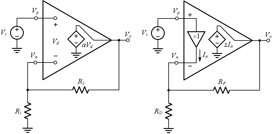
(a) (b)
Figure 1. Noninverting amplifier using the idealized model of (a) the VFA and (b) the CFA.
By inspection,
Equation (1)
Using KVL and the voltage divider formula, we write

Equation (2)
where β is called the feedback factor, defined as

Equation (3)
Substituting Equation (2) into Equation (1), collecting, and solving for the ratio Vo/Vi, we get

Equation (4)
where A is called the closed-loop gain. Let us put the above expression in the more insightful form
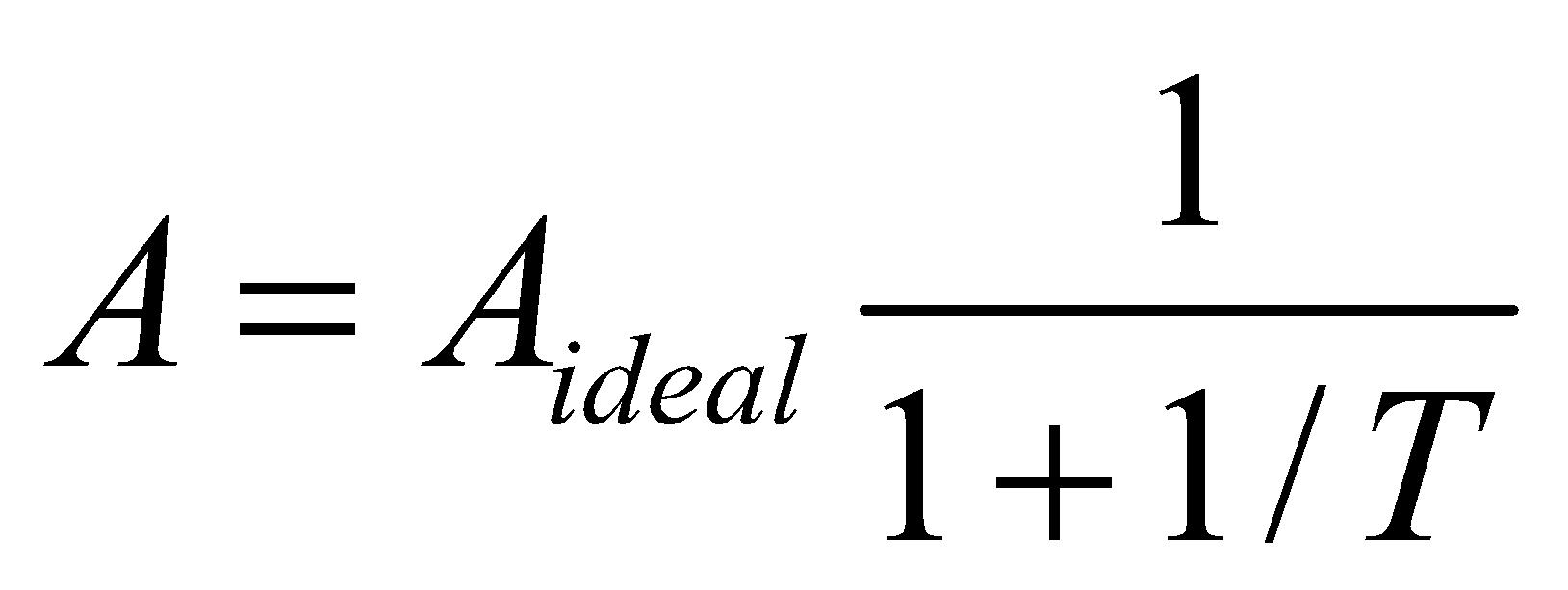
Equation (5)
where
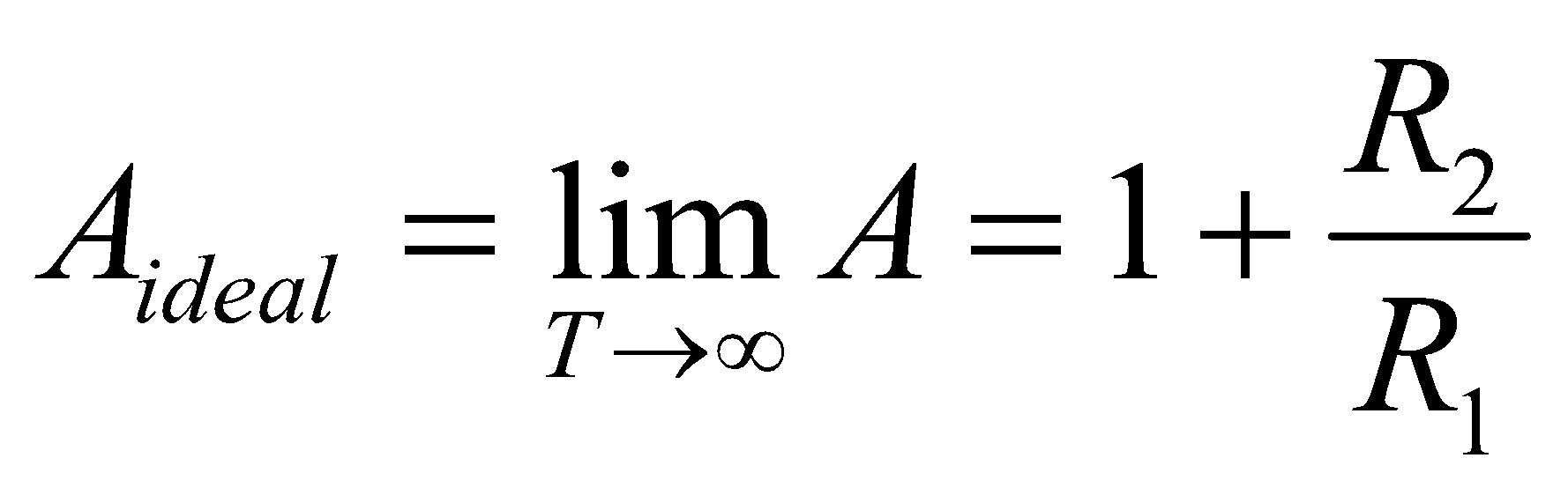
Equation (6)
and T is called the loop gain,

Equation (7)
This designation stems from the fact that Vd is first magnified by the open-loop gain a and is then attenuated by the feedback factor β, so the overall gain it experiences around the loop is T = aβ. (Note that T is dimensionless.)
Clearly, the limit T → ∞ is achieved for a → ∞.
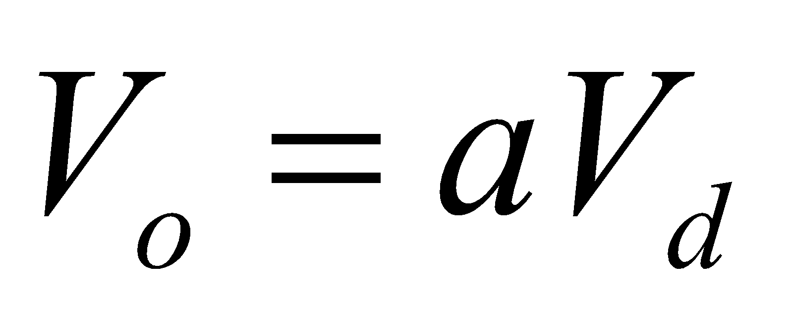
Example CFA: Current-Controlled Voltage Source
Turning next to Figure 1b, we observe that the CFA is modeled by means of a current-controlled voltage source (CCVS), with z representing the open-loop gain, in V/A or in Ω (for this reason, the CFA is also said to be a transimpedance amplifier).
The error signal is now the current In out of the unity-gain voltage buffer connected across the input pins. (How the device manages to respond to this current will become clearer in the next article on current-feedback amplifiers, when we look at its transistor-level schematic.)
In the idealized representation shown, this buffer is assumed to have infinite input impedance and zero output impedance.
By inspection,
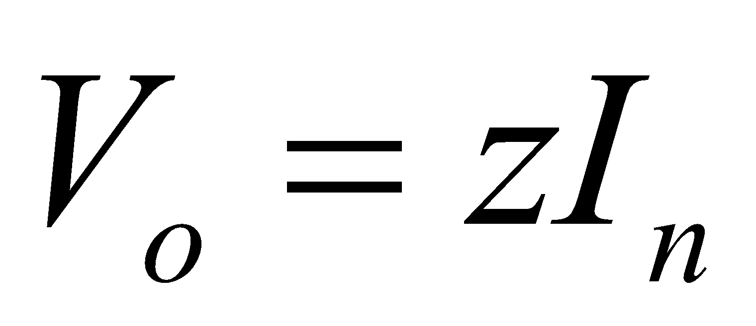
Equation (8)
Using KCL and Ohm’s law, and also exploiting the fact that the input buffer gives Vn = Vp = Vi, we write

Equation (9)
where the feedback factor is now defined as
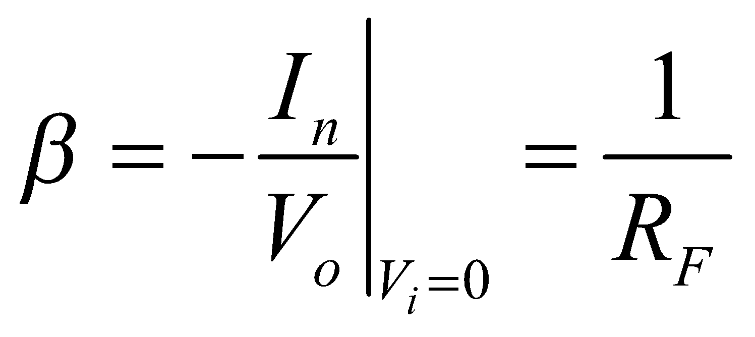
Equation (10)
and it is in A/V or Ω–1. Substituting Equation (9) into Equation (8), collecting, and solving for the ratio Vo/Vi, we get the closed-loop gain

Equation (11)
Let us put this expression in the already familiar form of Equation (5):

Equation (12)
where

Equation (13)
and the loop gain is now
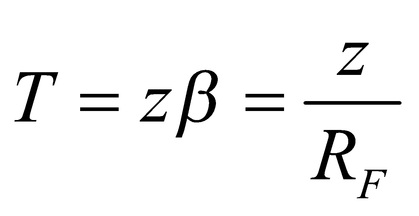
Equation (14)
This expression stems from the fact that In gets first multiplied by z to produce Vo, and then Vo gets divided by RF to produce again a current, so the overall gain around the loop is T = zβ. (Note that z is in V/A and β is in A/V, so T is dimensionless.) Clearly, the limit T → ∞ is achieved for z → ∞.
Comparing an Example CFA to an Example VFA
To better appreciate similarities and differences between the two op-amp types, consider the circuits of Figure 2, designed to amplify a 1.0 V input with Aideal = 10.0 V/V.
For the VFA circuit, we use Equation (7) to find T = 10,000. Then we find A via Equation (5), and Vd via Equation (1).
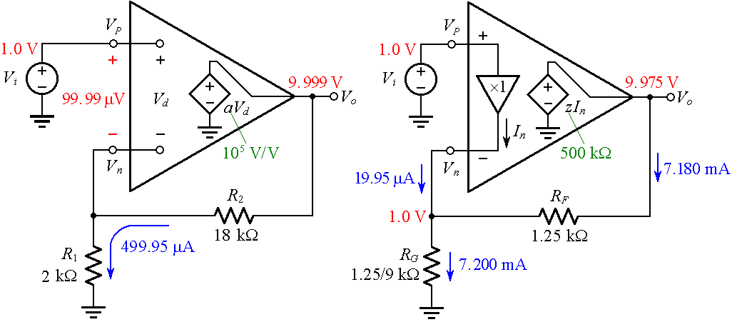
(a) (b)
Figure 2. Configuring (a) a VFA and (b) a CFA for noninverting amplification with Aideal = 10.0 V/V.
For the CFA circuit, we use Equation (14) to find T = 400. Then we find A via Equation (12), and In via Equation (8). Moreover, we calculate the currents through RG and RF via Ohm’s law.
We make the following observations:
- The VFA needs a (small) control voltage Vd to force the VCVS aVd to sustain the given Vo. Only in the idealized limit of a → ∞ do we get Vd → 0, or Vn = Vp.
- The CFA has Vn = Vp because of the unity-gain input buffer.
- The VFA draws zero current at both of its input pins.
- The CFA draws zero current at its noninverting input pin. However, the input buffer needs to source a (small) control current In out of the inverting input pin to force the CCVS zIn to sustain the given Vo. Only in the idealized limit of z → ∞ do we get In → 0.
AC Behavior of VFA and CFA Circuits
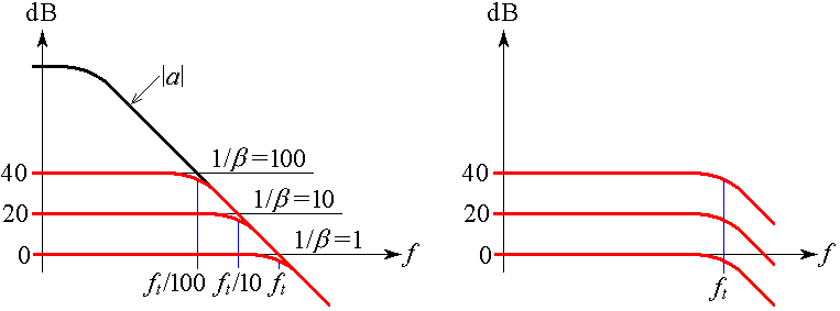
Most VFAs have an open-loop response a(jf) of the dominant-pole type depicted in Figure 3a, where a0 is the DC gain and fb is the dominant-pole frequency, also called the –3-dB frequency of |a(jf)|.
image2.png)
(a) (b)
Figure 3. Graphical visualization of the loop gain T as the difference between the open-loop gain curve and the 1/β curve for (a) the VFA circuit and (b) the CFA circuit of Figure 1.
This type of response is also said to exhibit a constant gain-bandwidth product (constant GBP), because at any point of the sloped portion of the curve the product GBP = |a|×f is constant. For instance, the popular 741 op-amp has a0 = 200,000 V/V and fb = 5 Hz, so its GBP = a0×fb = 1 MHz, and it remains constant all the way down the curve to the transition frequency ft, so called because it marks the point at which the amplifier transitions from amplifying to attenuating.
Now, writing T = aβ = a/(1/β), taking the logarithms, and multiplying by 20 to convert to decibels, gives

Equation (15)
indicating that we can visualize the decibel plot of |T| as the difference between the decibel plots of |a| and |1/β|, as shown in Figure 3a. Note that at the crossover frequency fx we have |T|dB = 0, or |T| = 1; moreover, |T| > 1 for f < fx, and |T| < 1 for f > fx. Because the GBP is constant, we can write (1+R2/R1)×fx = 1×ft, or

Equation (16)
Using Figure 3a, along with Equation (5), we construct the closed-loop ac response A(jf) as follows:
- At low frequencies, where |T| >> 1, we approximate A(jf) ≅ Aideal.
- At high frequencies, where |T| << 1, we approximate A(jf) ≅ AidealT = (1+R2/R1)a(jf)R1/(R1+R2) = a(jf).
- The borderline frequency fx at which |T| = 1 approximates the –3-dB frequency of |A(jf)|.
The above procedure is shown in Figure 4a for three values of Aideal (0, 20, and 40 dB, corresponding to 1, 10, and 100 V/V).
(a) (b)
Figure 4. Comparing the closed-loop gains of (a) the VFA and (b) the CFA noninverting amplifiers for three different values of Aideal (0, 20, and 40 dB, corresponding to 1, 10, and 100 V/V).
Note that as we increase Aideal by raising the R2/R1 ratio, the –3-dB frequency decreases in proportion, by Equation (16), so the VFA circuit is said to exhibit a gain-bandwidth tradeoff.
Turning next to the CFA case of Figure 3b, we observe that the open-loop response z(jf) of a CFA is also of the dominant-pole type, with z0 as the dc gain and fb as the dominant-pole frequency. Since z is in V/A or Ω, we can no longer express it in decibels; however, we still use logarithmic scales, after which Equation (14) indicates that we can visualize |T| as the difference between the logarithmic plots of |z| and |1/β|, as depicted in Figure 3b.
We now see an inherent advantage of the CFA: Since its crossover frequency ft depends only on RF (rather than on 1 + RF/RG), we can keep RF fixed and establish different values of Aideal by varying RG. As illustrated in Figure 4b, all closed-loop responses now exhibit the same –3-dB frequency.
Summary
We can summarize our comparison of voltage-feedback amplifiers and current-feedback amplifiers via two additional bullets:
- The VFA noninverting amplifier is constrained by a gain-bandwidth tradeoff.
- The CFA noninverting amplifier is relatively free from a gain-bandwidth tradeoff, since its closed-loop gain can be set independently of frequency via RG.
An additional advantage of CFAs compared to VFAs is the absence of slew-rate limiting, a feature that will be investigated in the next article, along with real-life departures from the idealized model of Figure 1b.
Related Content