Facebook
 Google
 GitHub
 Linkedin
Characteristics of Current-Feedback Op-Amps: Benefits of CFA Design vs. VFAs
In this article, we’ll take a more detailed look at the functionality and characteristics of current-feedback amplifiers.
In this article, we’ll take a more detailed look at the functionality and characteristics of current-feedback amplifiers (CFAs).
A current-feedback amplifier is a form of op-amp which most commonly serves as the error amplifier of a negative-feedback circuit where the input error is a current.
In this article, we'll talk about the step responses, slew rates, input buffers of CFAs.
CFA Series
This article is part of a series. Though this article is designed to be useful on its own, you may consider reading the preceding part before continuing.
The rest of the series can be found here:
- Part I: Introduction to the CFA: Current-Feedback Amplifiers vs. Voltage-Feedback Amplifiers
- Part II: Characteristics of Current-Feedback Op-Amps: Benefits of CFA Design vs. VFAs
- Part III: Applications and Limitations of the Current-Feedback Amplifier: Dual CFAs and Composite Amplifiers
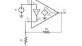
In the previous article, we highlighted some unique features of the current-feedback amplifier (CFA) using the idealized model (presented as Figure 1b in the previous article):
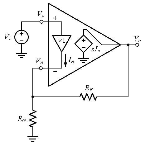
Figure 1. A noninverting amplifier using the idealized model of the CFA
We now wish to investigate how a practical CFA lives up to the above ideal expectations.
It turns out that a primary source of deviation from the ideal is the fact that the input buffer exhibits a non-zero output impedance rn, so we shall now work with the more realistic model of Figure 2a.
(a) (b)
Figure 2. Investigating the effect of the input buffer’s output resistance rn upon the feedback factor ß.
We note that the following equations still hold from when we first introduced them in the previous article (where they were presented as Equations (8) and (9). We'll repeat them here for convenience:
Equation (1)
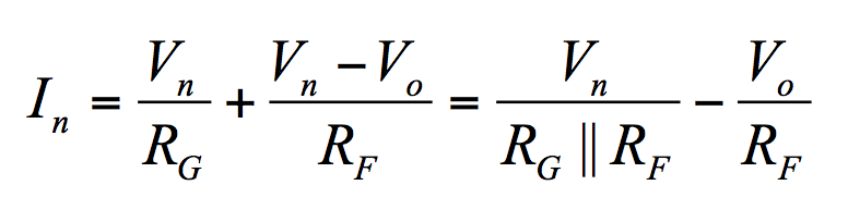
Equation (2)
However, we now have Vn ≠ Vp because of the voltage drop across rn. In fact, Ohm’s law gives Vp – Vn = rnIn, or, if we recall that Vp = Vi,
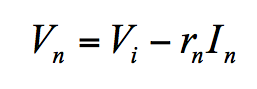
Equation (3)
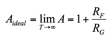
Substituting Equation (3) into Equation (2), we eliminate Vn. Collecting for In and then substituting into Equation (1), we eliminate In to obtain an expression involving only Vo and Vi. Collecting once again and solving for the ratio Vo/Vi gives the closed-loop gain A, which we express as
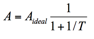
Equation (4)
where
Equation (5)
and
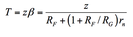
Equation (6)
The presence of rn has no effect upon Aideal. However, it raises the 1/ß curve, and in so doing it reduces both the loop gain T and the crossover frequency fx, compared to the idealized case rn = 0, for which T = z/RF and fx = ft. (Henceforth, we visualize ft as the crossover frequency extrapolated to the limit rn → 0.)
Example: The Effect of rn in a DC Circuit
To get an idea, let us rework the DC example from the first article (presented there as Figure 2b)—but with rn = 40 Ω in place.
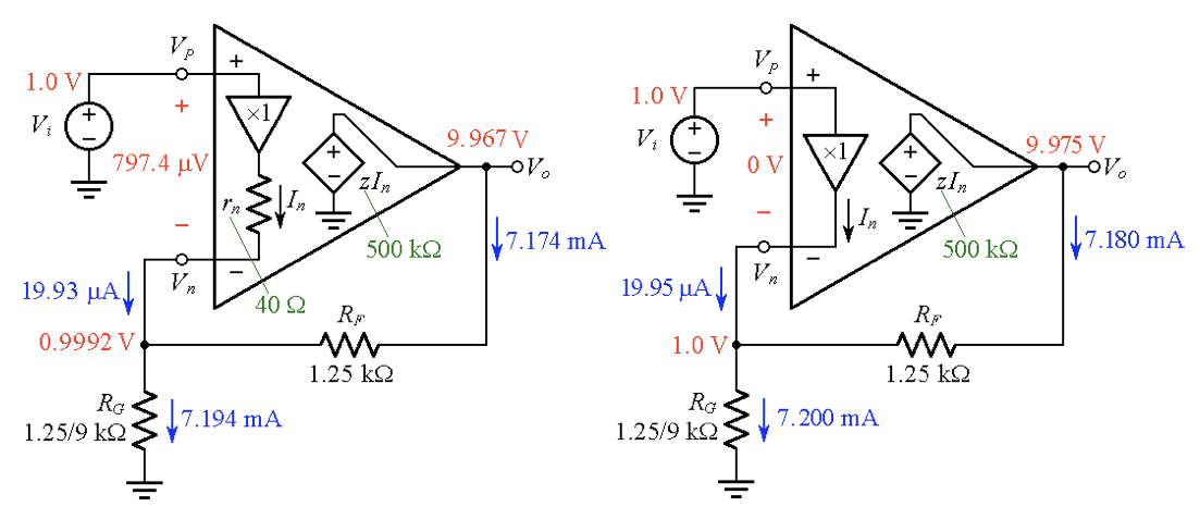
(a) (b)
Figure 3. Visualizing DC voltages and currents for the cases (a) rn = 40 Ω and (b) rn = 0.
Using Equation (6), we find T = 303.03 (a drop from T = 400 from the circuit in the previous article). Then we find A via Equation (4), In via Equation (1), Vp – Vn via Ohm’s law, and Vn via Equation (3).
Moreover, we calculate the currents through RG and RF via Ohm’s law. The results are visualized in Figure 3a (for easy comparison, the example from the previous article is repeated in Figure 3b).
It is apparent that the most noticeable effects of rn are to cause Vn ≠ Vp, and also to contribute a slight reduction in Vo due to the decrease of T from 400 to 333.
The Closed-Loop AC Response
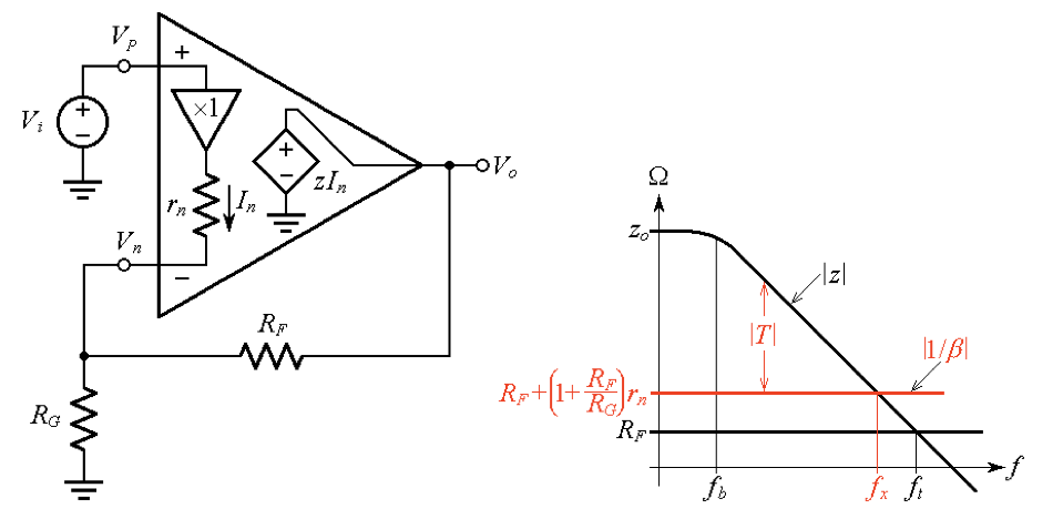
We now wish to take a closer look at the crossover frequency fx of Figure 2b.
As discussed in our comparison of CFAs and VFAs, this frequency approximates the –3-dB frequency of the closed-loop response A(jf).
Since z(jf) is of the dominant-pole type, the GBP = |z| × f is constant on the sloped portion of the curve, so we can write
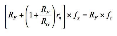
Equation (7)
Solving for fx gives, after simplification,
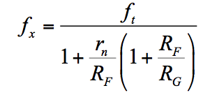
Equation (8)
This expression is reminiscent of the VFA equation we presented in the previous article as Equation (16), except for the presence of the term rn/RF, which is a well-designed CFA is such that rn/RF << 1. Consequently, there is a bit of gain-bandwidth tradeoff also in CFAs, but this is much lighter than in VFAs. For instance, in the circuit with rn = 40 Ω and RF = 1.25 kΩ of Figure 3a, adjusting RG for (1 + RF/RG) = 1, 10, and 100 V/V, we get fx = ft/1.032, ft/1.32, and ft/4.2, as shown in Figure 4.
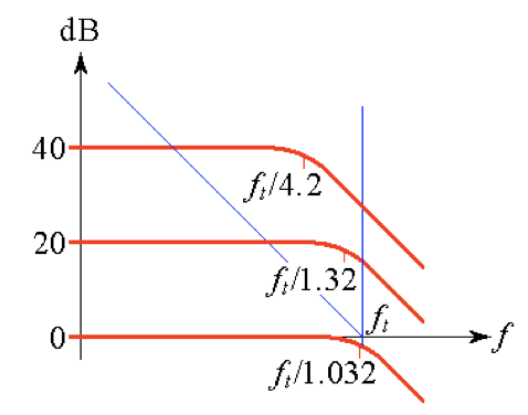
Figure 4. Illustrating the effect of rn = 40 Ω upon the closed loop bandwidth for Aideal = 0, 20, and 40 dB.
These compare quite favorably with the VFA values of fx = ft, ft/10, and ft/100.
Step Responses
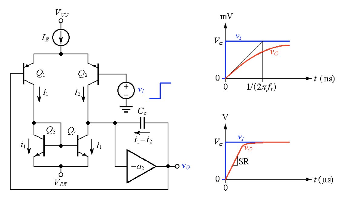
We conclude our VFA–CFA comparison by taking a look at the step responses. Turning first to the VFA, we use the simplified model of Figure 3a, which is typical of many VFAs. We shall focus on the input stage (Q1 through Q4), so we lump together all subsequent stages into a single inverting stage assumed to have gain –a2. (The purpose of Cc is to provide an open-loop response of the dominant-pole type.)
The bias current IE splits between Q1 and Q2 to form i1 and i2 (for simplicity, we are assuming negligible BJT base currents). Now, i1 flows into the diode-connected transistor Q3, and since Q4, its matched twin, is subjected to the same base-emitter voltage drop as Q3, then Q4 will just mirror Q3’s current i1, this being the reason why the Q3-Q4 pair is said to form a current mirror. By KCL, the capacitor current is i1 – i2.
(a) (b)
Figure 5. (a) Simplified VFA model connected as a voltage follower, and step responses: small-signal exponential transient (top), and slew-rate-limited ramp (bottom).
When vO = vI, the circuit is said to be balanced because i1 = i2, so the capacitor current is i1 – i2 = 0. If we now apply an input step of suitably small magnitude Vm, we are making Q2 less conductive and Q1 more conductive, thus unbalancing the circuit to give i1 – i2 > 0. This will cause Cc to charge up and produce a transient at the output, which in turn will gradually reduce the initial imbalance via negative feedback. Just as in the case of a plain R-C network, we get an exponential transient, and its time constant is τ = 1/(2πft), as shown in Figure 5b, top. (For the 741 op-amp, which has ft = 1 MHz, we have τ = 159 ns.)
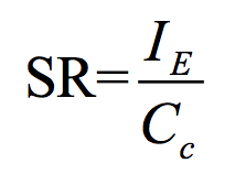
Now, if we increase Vm, we’ll reach a point at which all of IE will be diverted to Q1, causing Cc to charge at a constant rate, as shown in Figure 5b, bottom. This is the maximum rate at which vO can swing. Aptly called the slew rate (SR), it is easily found via the capacitance law to be
Equation (9)
For the 741 op-amp, which uses IE = 20 µA and Cc = 30 pF, we get SR = 0.67 V/µs. The maximum amplitude Vm before the onset of slew-rate limiting is obtained by equating the initial slope of the exponential transient to SR, or Vm/τ = SR, which gives Vm = IE/(Cc×2πft ). For the 741 op-amp, we get Vm = 116 mV. Under slew-rate limiting, vO ramps up at a constant rate until it comes within 116 mV of the final value, after which it completes the rest of the transient in an exponential fashion.
Step Responses of a CFA
Let us now turn to the step response of the CFA, but using the circuit schematic of Figure 6, which will also help us better understand the CFA’s overall internal workings.
We make the following observations:
- The function of Q1 and Q2 is to form a low-output-impedance push-pull stage, while Q3 and Q4 provide a Darlington-type function to increase the input impedance. Also, the base-emitter voltage drops of Q3 and Q4 are meant to compensate in a complementary fashion for those of Q1 and Q2 so as to eliminate any DC offset between nodes Vn and Vp. This is the input buffer, represented at the bottom of Figure 6 as a unity-gain buffer with output resistance rn.
- In negative-feedback operation, the current In drawn by the external feedback network splits between Q1 and Q2 such that In = I1 – I2, by KCL (again, we are assuming negligible BJT base currents).
- The trios Q5-Q6-Q7 and Q8-Q9-Q10 form high-quality current mirrors of the so-called Wilson type, for the purpose of mirroring I1 and I2, respectively, in and out of an important node called the gain node (GN). Denoting GN’s equivalent impedance towards the ground as z, it is apparent that the net current into z is a replica of the inverting-input current In itself, so we model the entire action of the mirrors by means of a single unity-gain current-controlled current source (CCCS), as shown at the bottom.
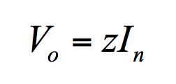
- BJTs Q11 through Q14 form the output buffer, identical in topology to the input buffer Q1 through Q4 (for simplicity, its output resistance ro is usually ignored because it plays a much lesser role than rn). Thanks to this buffering action, we write Vo = zIn and we model the CFA with a CCVS as in Figure 1.
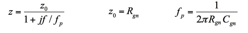
- The impedance is modeled as the parallel combination of equivalent resistance Rgn and capacitance Cgn, or z = Rgn||[1/(j2πfCgn)]. Expanding,
Equation (10)
With reference to Figure 2b, we can easily find an expression for ft by imposing z0 × fp = RF × ft, obtaining
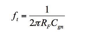
Equation (11)
In a well-designed CFA, Rgn is on the order of 106 Ω, Cgn is in the picofarad range, and RF is on the order of 103 Ω. The time constant τ = (RFCgn) is then in the nanosecond range.
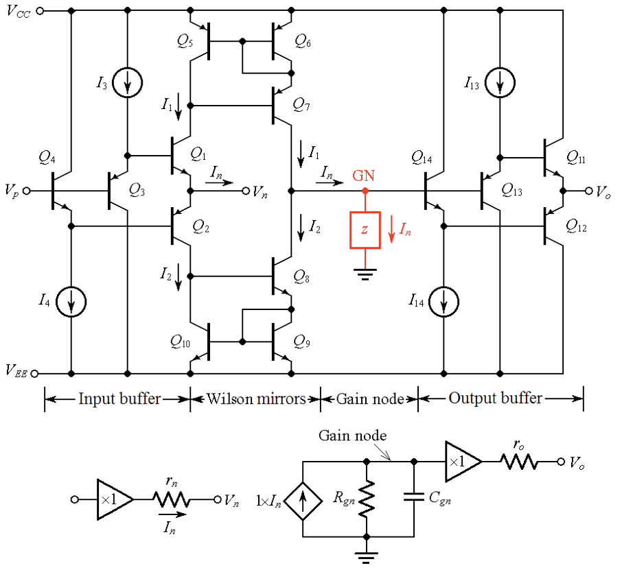
Figure 6. Circuit schematic of a CFA (top) and its constituent blocks (bottom).
We are now in the position to state that there is no slew-rate limiting in CFAs because the input buffer will deliver to GN whatever current it takes to ensure an exponential transient at the output, regardless of the input step size Vm. For instance, the circuit of Figure 3a, in response to an input step with Vm = 1 V, will provide an initial current of In = Vp/[rn + (RG||RF)] = 6.06 mA.
Were we to remove RG in order to operate the CFA as a unity-gain voltage follower with a 10 V input step, the initial current would be In = Vp/(rn + RF) = 7.75 mA, much larger than the maximum current IE = 20 µA available in the 741 op-amp!
CFAs are well suited to applications that might suffer from slew-rate-induced distortion and nonlinearity.
Continue reading in Part II: Benefits of CFA Design vs. VFAs.
Related Content