Facebook
 Google
 GitHub
 Linkedin
Applications and Limitations of the Current-Feedback Amplifier: Dual CFAs and Composite Amplifiers
In this article, we continue our study of the current-feedback amplifier. We’ll also look at a composite amplifier that combines the benefits of the voltage-feedback topology and the current-feedback topology.
In this article, we continue our study of the current-feedback amplifier. We’ll also look at a composite amplifier that combines the benefits of the voltage-feedback topology and the current-feedback topology.
Before continuing, please consider reviewing the information in the previous two articles on VFAs (voltage-feedback amplifiers) and CFAs (current-feedback amplifiers):
- Part I: Intro to CFAs: Current-Feedback Amplifiers vs. Voltage-Feedback Amplifiers
- Part II: Benefits of CFA Design vs. VFAs
Configuring a CFA: The Importance of Rf
In general, each node in a circuit contributes a pole frequency of the type
Equation (1)
where Rnode is the equivalent resistance presented by that node, and Cnode is its stray capacitance towards ground.
In the last article, we considered a specific CFA schematic, shown below:
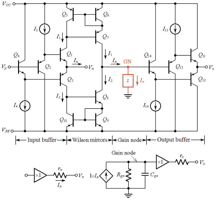
Figure 1. Circuit schematic of a CFA (top), and its constituent blocks (bottom).
Here, each node other than the gain node is such that Rnode << Rgn, where Rgn is the equivalent resistance presented by the gain node. As a result, the open-loop transimpedance gain z(jf) is dominated by the gain-node pole fp = 1/(2πRgnCgn), with all remaining poles typically clustered at least some 3–4 decades above this dominant pole.
The optimum value of RF specified in datasheets is the result of a compromise between the desire to keep the 1/ß curve as low as possible to maximize the loop gain T, and the need to avoid pushing its crossover frequency fx into the region of excessive phase lag due to the higher-frequency poles.
Thus, when configuring a CFA for voltage-follower operation, we must include RF in its feedback path, as shown in Figure 2(a).
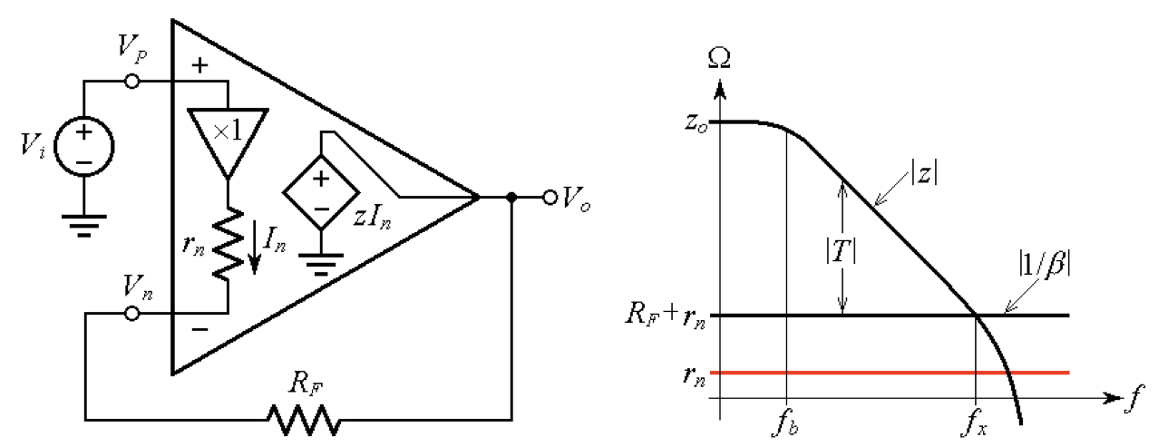
(a) (b)
Figure 2. (a) A voltage-follower CFA, and (b) its 1/β curve. Using a wire instead of RF would destabilize the circuit and cause it to oscillate.
Using a plain wire, as in the case of a VFA, would push down the 1/β curve till it coincides with rn and crosses the |z| curve in a region of excessive phase shift, where there would be no phase margin left, and the circuit would surely oscillate.
So long as a CFA is equipped with the proper RF, it can be used in virtually all the resistive applications that are typical of the VFA, such as inverting and non-inverting amplifiers, summing amplifiers, difference amplifiers, and I-V converters.
It works well also in filter applications that utilize op amps with resistive feedback.
Stability Issues with CFAs: Integrator Applications
Despite the versatility of a CFA with an appropriate RF, using the CFA as the popular Miller integrator is not allowed on account of stability considerations. To see why, refer to Figure 3(a), where we note that since the feedback element is the impedance ZF = 1/(j2πfC), we now have 1/β = ZF + rn.
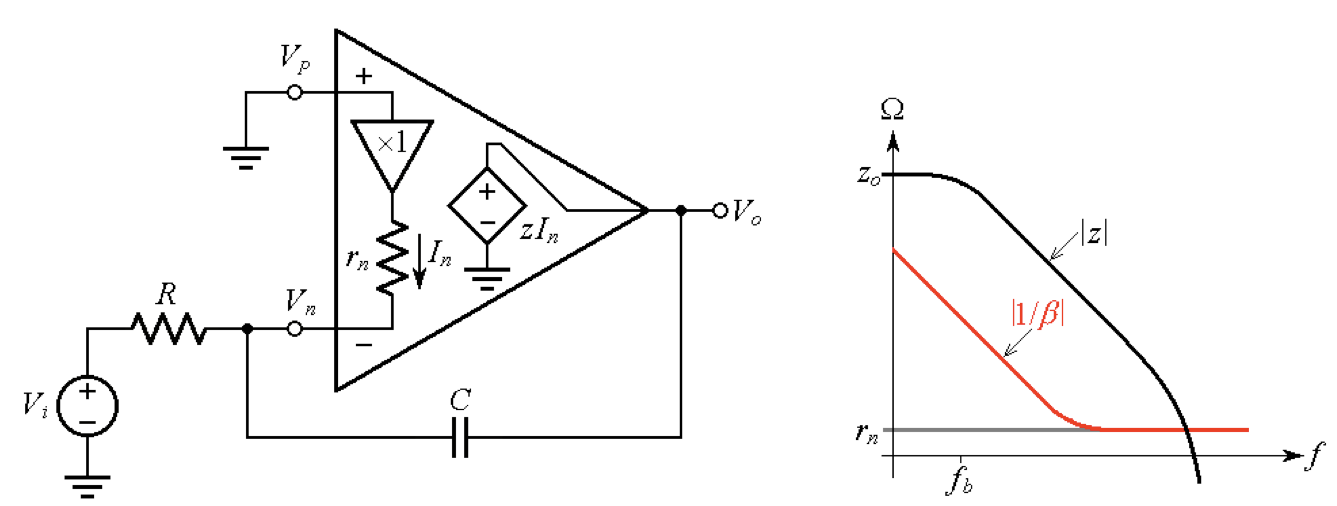
(a) (b)
Figure 3. (a) A Miller integrator and (b) its 1/β curve.
At low frequencies, where |ZF| >> rn, we have |1/β| → 1/(2πfC), and at high frequencies, where |ZF| << rn, we have |1/β| → rn. As depicted in Figure 3(b), the crossover frequency is again in a region of excessive phase shift, where no phase margin is left and the circuit is likely to oscillate.
How to Gain Stability by Using a Dual CFA
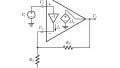
The alternative realization of the above concept uses two CFAs to provide the integration function without destabilizing either CFA:
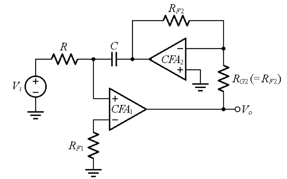
Figure 4. Integrator realization using a dual CFA.
Here, CFA2 works as a unity-gain inverting amplifier, driving the capacitor’s right plate with the voltage –Vo. The current through RF1 = Vo/z1, (where z1 is the open-loop gain of CFA1) is vanishingly small, so we assume the non-inverting input of CFA1 to be at zero potential.
This allows us to write, by KCL,
Equation (2)
giving the transfer function,
Equation (3)
This is the transfer function of a non-inverting integrator having fo as its unity-gain frequency. This circuit, easily realizable with a dual CFA IC, enjoys also the advantage of active frequency compensation [1], a highly desirable feature for coping with Q-enhancement issues in dual-integrator-loop filters.
How to Counteract Phase Lag in a CFA
There are situations in which a (small) feedback capacitance is allowed, and this is when it is necessary to counteract the phase lag arising from the presence of a substantial stray capacitance at the inverting input.
A typical example is the I-V conversion of a current-output digital-to-analog converter (DAC), which appears as a current sink Ii with a parallel stray capacitance Cs on the order of tens or even hundreds of picofarads, as depicted in Figure 5(a).

(a) (b)
Figure 5. (a) I-V converter, and (b) investigating its stability via linearized Bode plots: subscript u stands for uncompensated (CF = 0) and subscript c for compensated (CF in place).
Ideally, the circuit would give Vo = RFIi. We wish to assess the effect of Cs graphically. We observe that at low frequencies, where Cs acts as an open circuit, we still have 1/β → RF + rn. The presence of Cs starts to be felt when its impedance |Zs| becomes equal to the resistance seen by Cs itself, which is RF||rn. This occurs at the frequency fp such that |1/(j2πfpCs)| = RF||rn, or
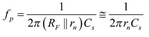
Equation (4)
where the fact that rn << RF has been exploited.
Past fp, the 1/β curve starts to rise, indicating that fp is a zero frequency for 1/β, and therefore a pole frequency for the loop gain T = zβ, where z is the open-loop gain of the CFA. This pole erodes the phase margin of the circuit, bringing it on the verge of oscillation, so we need some form of frequency compensation.
To counteract the phase lag due to Cs we introduce phase lead via a feedback capacitor CF, as shown. A good starting point is to break the 1/β curve right at the crossover frequency fx, which will result in a phase margin of about 45°.
Considering that rn << RF, we can approximate the crossover frequency between the RF + rn curve and the z curve as ft. Then fx is the geometric mean of fp and ft, so imposing
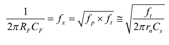
Equation (5)
and solving for CF gives
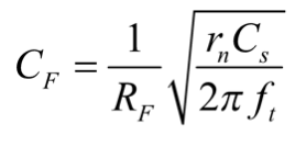
Equation (6)
If a greater phase margin than the estimated 45° is desired, it can be achieved by suitably increasing the value of CF. This task is best done empirically by observing the step response with an oscilloscope and raising CF until the overshoot is lowered to an acceptable value.
The Composite Amplifier: The Best of CFAs and VFAs
The fast dynamics (wide bandwidths as well as high slew rates) and low-distortion characteristics of CFAs make them suited to high-speed applications such as video systems, radar systems, IF and RF stages, DSL, and automated test equipment applications.
VFAs, on the other hand, offer better DC characteristics (low input offset voltage and bias currents), lower noise, and higher loop gains, so they are better suited to precision applications.
Figure 6 shows a composite amplifier that offers the best of both worlds.
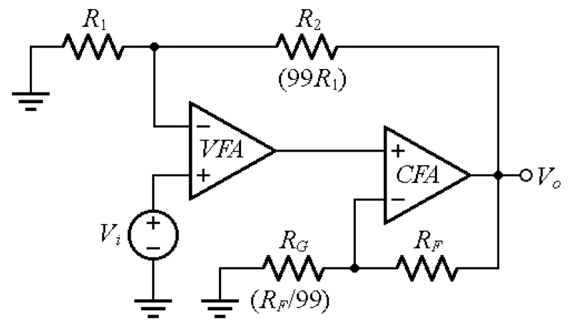
Figure 6. A composite amplifier enjoying the best of both the VFA and the CFA worlds.
The circuit uses a VFA with a constant gain-bandwidth product (GBP) of 10 MHz to achieve a closed-loop gain of 100 V/V with a closed-loop bandwidth of also 10 MHz. Were it to act alone, the VFA would be capable of a bandwidth of only (10 MHz)/100 = 100 kHz. However, cascading it with a much faster CFA with a gain of 100 will trick the VFA into amplifying only by 1 V/V, that is, into acting as a mere voltage follower, whose closed-loop bandwidth we know to coincide with its GBP, in turn coinciding with ft.
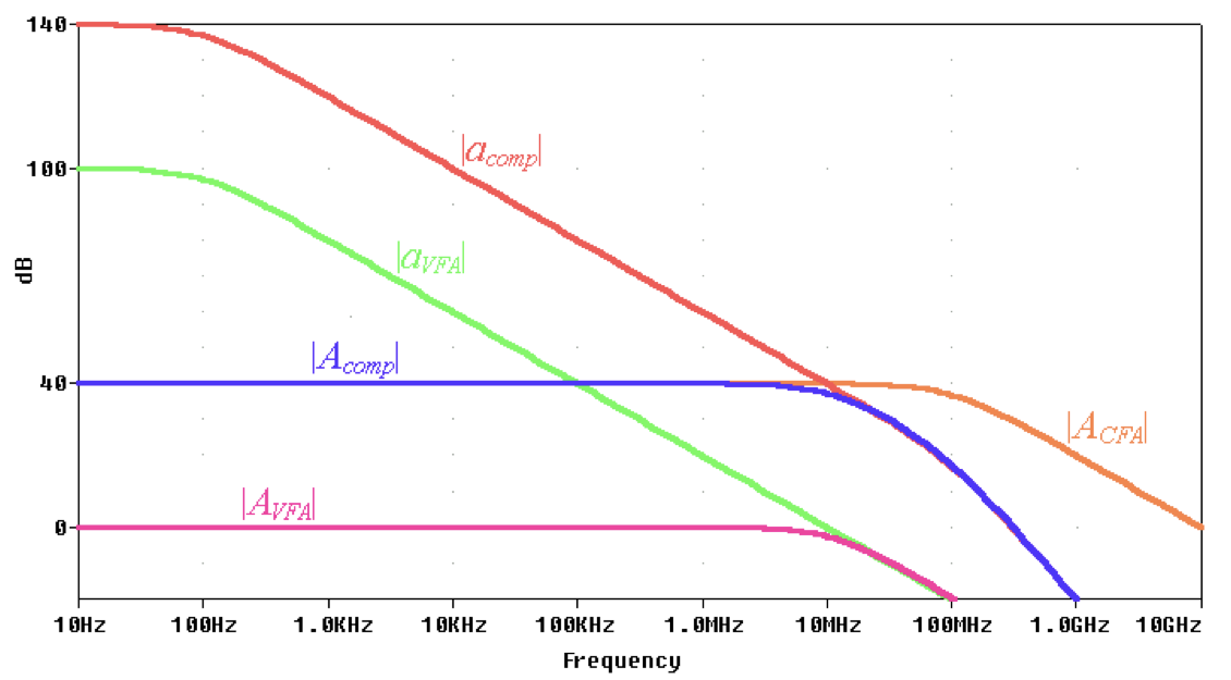
Figure 5. Bode plots for the composite amplifier of Figure 6. Cascading the VFA with a CFA having a closed-loop gain ACFA of 40 dB shifts the VFA’s open-loop gain aVFA upwards also by 40 dB, thus resulting in the composite open-loop gain acomp, and in the composite closed-loop gain Acomp. Note how the VFA is tricked into acting as a unity-gain voltage follower with closed-loop gain AVFA of 0 dB.
To avoid destabilizing the VFA by introducing any substantial delay within its feedback loop, the closed-loop bandwidth of the CFA should be much higher (by, say, a decade or more) than the GBP of the VFA, an easily achievable goal with the faster CFAs.
The circuit enjoys the better input characteristics of the VFA (low input DC errors and noise) as well as the maximum achievable loop gain while providing the high slew rate and lower distortion of the CFA. Note also that any overheating by the output stage of the CFA will never reach the input stage of the VFA, thus reducing significantly the effects of input thermal drift.
In this article, we continued our investigation of the CFA circuit topology. We discussed how the CFA can be used in the resistive applications often suited to VFAs (i.e., inverting and non-inverting amplifiers, summing amplifiers, difference amplifiers, and I-V converters).
We also looked at the limits to this concept as stability prevents the CFA from being appropriate for Miller integrator applications but how integration may be achieved via the use of a dual CFA.
Finally, we explored the concept of the composite amplifier, which combines the strengths of two separate amplifiers to attain performance not possible with a single amplifier alone.
References
[1] http://online.sfsu.edu/sfranco/BookOpamp/OpampsJacket.pdf
Related Content