Facebook
 Google
 GitHub
 Linkedin
A Four-Channel RS-422 Differential Line Receiver Module
This project brief describes how to build and use a four-channel differential line receiver module for balanced RS-422 and RS-485 data links.
This design is for a quadruple differential line receiver designed for balanced or unbalanced digital data transmission over RS-422 and RS-485 links. It accepts four independent differential input pairs and converts them to single-ended digital outputs suitable for direct connection to a microcontroller or bus-organized system. It also complements our previous project, a four-channel RS-422 differential line driver.
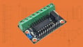
The fully assembled board is shown in Figure 1. All four receivers share a common enable function with both active-high and active-low control inputs, and the 3-state outputs allow safe multi-device bus sharing.
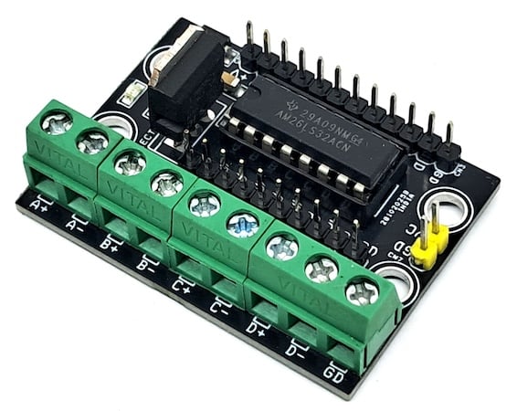
Figure 1. Assembled AM26LS32 quadruple differential line receiver module.
Specs and Features
- Power input: 7 to 18 VDC
- On-board 5 V regulation via LM7805
- ±7 V common-mode range with ±200 mV sensitivity
- Input hysteresis: 60 mV typical
- 3-state outputs — bus-compatible
- Fail-safe: open inputs default to logic high
- Common enable with active-high and active-low inputs (solder-jumper selectable)
- Four 120 Ω on-board termination resistors
- On-board power LED
- Screw terminals for twisted-pair input cables (5.08 mm pitch)
- 8-pin output header for microcontroller interfacing (2.54 mm pitch)
- PCB dimensions: 55.25 mm × 37.47 mm
- Four 3 mm mounting holes
How It Works
The heart of the design is the AM26LS32 IC from Texas Instruments, a quad differential line receiver in a DIP-16 package with ±7 V common-mode range and 60 mV of input hysteresis. As illustrated in the logic diagram of Figure 2, the AM26LS32 contains four independent differential line receivers. Each differential line receiver accepts a balanced input pair and produces a single-ended TTL/CMOS-compatible output.
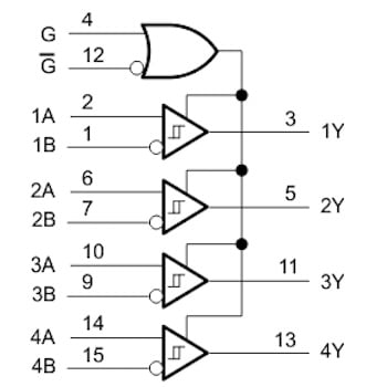
Figure 2. Logic diagram for AM26LS32 quadruple differential line receiver IC. Image used courtesy of Texas Instruments
The receiver compares the voltage difference between each A and B input. If A exceeds B by more than the sensitivity threshold (±200 mV), the output goes high. If B exceeds A, the output goes low. The 60 mV of built-in hysteresis suppresses noise-induced toggling near the threshold.
All four receivers share a single enable pair (EN low / EN high) controlled through the J1 and J2 solder jumpers on the bottom of the board. When disabled, all outputs enter the high-impedance (3-state) condition, allowing the module to be safely connected to a shared bus.
The fail-safe circuit ensures that any open or undriven input defaults to a logic-high output, avoiding undefined states when cables are disconnected.
Power conditioning is handled by the LM7805 linear regulator, which accepts the 7 V to 18 V supply on CN8 and delivers a regulated 5 V rail. D2 (1N4007) provides reverse-polarity protection. Decoupling capacitors C1 (100 nF) and C2 (10 µF) suppress high-frequency and low-frequency noise on the 5 V rail. The power LED (D1) with series resistor R5 (1 kΩ) gives a visual indication that 5 V is present.
Cables and Termination
Proper cable termination is essential for reliable RS-422 and RS-485 systems. Because RS-422 allows only one driver on the bus, termination is placed only at the receiver end of the cable. RS-485 typically requires termination at both ends. This module includes a 120 Ω termination resistor on each differential input pair, matched to the characteristic impedance of standard twisted-pair cable.
Common termination approaches include parallel termination (120 Ω resistor directly across the line at the receiver), AC termination (series RC network to reduce DC loading), and split termination (two resistors to a mid-supply reference). The appropriate method depends on data rate, cable length, and DC power budget. For most RS-422 applications using 100 ft (30 m) or less of 24-AWG twisted-pair cable, the on-board 120 Ω parallel termination is sufficient.
Schematic and Bill of Materials
Figure 3 shows the schematic for the four-channel RS-422 differential line receiver module.
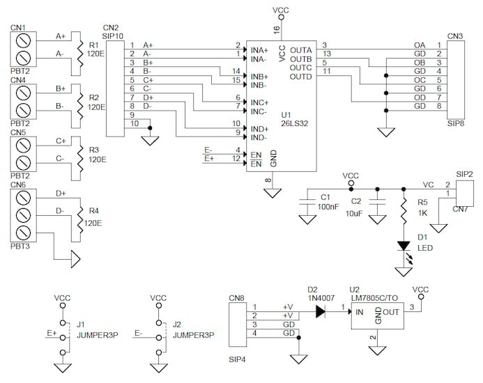
Figure 3. AM26LS32 quadruple differential line receiver module schematic.
The bill of materials is provided in Table 1.
Table 1. BOM for the AM26LS32 quadruple differential line receiver module.
| REF | DESCRIPTION | QTY | MFG | SUPPLIER | PART NO. |
| CN1, CN4, CN5 | 2-Pin Screw Terminal, 5.08 mm Pitch | 3 | Phoenix | DigiKey | 277-1247-ND |
| CN2 | 10-Pin Male Header, 2.54 mm Pitch | 1 | Würth | DigiKey | 732-2670-ND |
| CN3 | 8-Pin Male Header, 2.54 mm Pitch | 1 | Würth | DigiKey | 732-5321-ND |
| CN6 | 3-Pin Screw Terminal, 5.08 mm Pitch | 1 | Phoenix | DigiKey | 277-1248-ND |
| CN7 | 2-Pin Male Header, 2.54 mm Pitch | 1 | Würth | DigiKey | 732-5315-ND |
| CN8 | 4-Pin Male Header, 2.54 mm Pitch | 1 | Würth | DigiKey | 732-5317-ND |
| C1 | 100 nF / 25 V Ceramic SMD 0805 | 1 | Yageo / Murata | DigiKey | |
| C2 | 10 µF / 25 V Ceramic SMD 0805 | 1 | Yageo / Murata | DigiKey | |
| D1 | LED, Red | 1 | Osram | DigiKey | 475-1278-1-ND |
| D2 | 1N4007 SMD | 1 | Diode Inc. | DigiKey | S1MBDITR-ND |
| J1, J2 | PCB Solder Jumper, 3-Position | 2 | — | — | |
| R1, R2, R3, R4 | 120 Ω, 5% SMD 1206 | 4 | Yageo / Murata | DigiKey | |
| R5 | 1 kΩ, 5% SMD 0805 | 1 | Yageo / Murata | DigiKey | |
| U1 | AM26LS32 Quad Differential Receiver, DIP-16 | 1 | Texas Instruments | DigiKey | 296-1376-5-ND |
| U2 | LM7805C Voltage Regulator, TO-220 | 1 | Lumimex | DigiKey | 4491-L7805-ND |
Connections
The connection diagram in Figure 4 shows all input and output assignments.
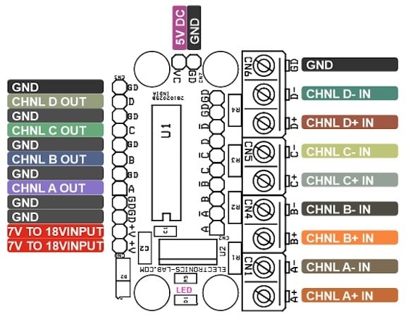
Figure 4. AM26LS32 module connection diagram.
CN1 — Channel A Differential Input (2-pin screw terminal, 5.08 mm pitch):
- Pin 1 = Channel A+ Input
- Pin 2 = Channel A− Input
CN4 — Channel B Differential Input (2-pin screw terminal, 5.08 mm pitch):
- Pin 1 = Channel B+ Input
- Pin 2 = Channel B− Input
CN5 — Channel C Differential Input (2-pin screw terminal, 5.08 mm pitch):
- Pin 1 = Channel C+ Input
- Pin 2 = Channel C− Input
CN6 — Channel D Differential Input (3-pin screw terminal, 5.08 mm pitch):
- Pin 1 = Channel D+ Input
- Pin 2 = Channel D− Input
- Pin 3 = GND
CN2 — SIP-10 Header (optional — Do Not Install):
- Not populated in standard configuration
CN3 — Output Header (8-pin male, 2.54 mm pitch):
- Pin 1 = Output A
- Pin 2 = GND
- Pin 3 = Output B
- Pin 4 = GND
- Pin 5 = Output C
- Pin 6 = GND
- Pin 7 = Output D
- Pin 8 = GND
CN7 — 5 V Power Tap (2-pin male header, 2.54 mm pitch):
- Pin 1 = GND
- Pin 2 = 5 V DC
CN8 — Power Input (4-pin male header, 2.54 mm pitch):
- Pins 1, 2 = 7 V to 18 V DC Input
- Pins 3, 4 = GND
J1, J2 — Enable Solder Jumpers (under PCB):
- J1 = Active-low enable (EN−)
- J2 = Active-high enable (EN+)
D1 — Power LED:
- Illuminates when 5 V is present on the board
PCB Files
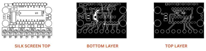
Figure 5. PCB layout: top silk screen, bottom copper layer, top copper layer.
Four-Channel Differential Line Receiver Module — Gerber Files
You can download the layout files for this project here:
Differential Line Receiver Gerber Files
Except where noted, all images used courtesy of Rajkumar Sharma