 Facebook
 Google
 GitHub
 Linkedin
PCB Layout for an Arbitrary Waveform Generator
In this article we’ll discuss the PCB layout for a custom-designed arbitrary waveform generator board.
In this article, we’ll discuss the PCB layout for a custom-designed arbitrary waveform generator (AWG) board.
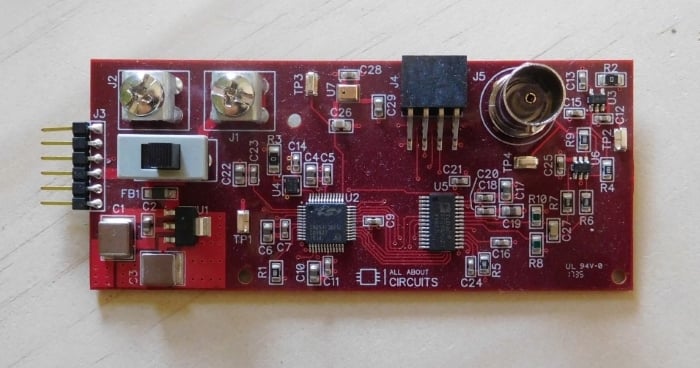
This is the fourth article that I’ve written about the design of my AWG PCB. This is what the board looks like:
The other three articles cover the microcontroller, the DAC, and the DAC’s output circuitry. Now it’s time to discuss the layout; after this article, we’ll consider the technical introduction complete, and we’ll move on to the actual projects.
The Basics
This PCB, like almost all of my PCBs, is a four-layer board. In my opinion, it is not wise to restrict yourself to two layers unless you’re dealing with a very simple circuit or you really need to cut costs.
The four-layer arrangement is beneficial in terms of routing and performance: routing, because via connections to internal planes almost completely eliminate power and ground traces; and performance, because the internal planes allow for low-resistance, low-inductance power and ground connections. The extra top-layer and bottom-layer real estate opened up by all the internal-plane connections come in very handy when you need to provide a generous copper area for improved thermal performance (for example, to make sure that your LDO or your motor driver doesn’t overheat and enter thermal shutdown).
The Power Supply
We might as well discuss the power supply circuit while we’re on the topic of thermal design.

You can see how all the power supply connections use large traces or copper pours. The AWG doesn’t have high current requirements, but the board house doesn’t give you a discount for using less copper, so you might as well opt for large (= low-resistance, low-inductance) traces if you have the room.
You can also see that I’ve made it very easy for heat to move away from the regulator (U1) and into the ambient environment or into other portions of the PCB. U1’s thermal tab is connected to a large copper pour, and this copper pour is shot through with vias that conduct heat down to the internal ground plane. If I were really worried about thermal issues I could also connect these vias to a copper pour on the bottom side of the board, but in this case, it would have been total overkill.
The Microcontroller
Here is the layout for the microcontroller portion of the board:

The decoupling capacitors (C4, C5, C6, C7, C9, C10, C11) are arranged around the perimeter of the chip, very close to their respective power pins and to the vias that connect the caps to the internal planes. Notice how the smaller cap is always closer to the power pin; this is because we rely more on the lower-value capacitor for high-frequency bypassing, and thus the first priority is minimizing the inductance and resistance between the smaller cap and the pin.
Note that U4, a 10 MHz MEMS oscillator, is also very close to the microcontroller’s clock input pin. It’s always a good idea to minimize the length of traces carrying high-frequency digital signals. First of all, there are noise benefits: a shorter, more direct trace reduces the amount of noise that would otherwise be coupled into adjacent traces, and a shorter trace also reduces electromagnetic interference (EMI) because it is less effective as an antenna. The second issue is related to transmission-line effects. Minimizing trace length is a simple way to avoid problems related to signal reflections. However, reflection is not a significant concern at frequencies in the 10 MHz range, unless you are dealing with long interconnections or a very large PCB.
The Parallel Bus
This next image shows the layout for the DAC; the microcontroller and DAC are arranged such that the 8-bit parallel data bus travels from the right side of the microcontroller to the left side of the DAC.

As you may have noticed, this is one of those annoying situations in which the pin configuration is the opposite of what you want: the DAC’s input pins move from bit 7 to bit 0 going downward, whereas the MCU’s output pins move from bit 7 to bit 0 going upward. I couldn’t remedy this by re-assigning the microcontroller pins because I wanted the data bits to correspond to the actual bits of the Port 2 register (so that I could write a full byte to the DAC without moving bits around). So I ended up with some awkward routing, but nothing terrible.
It’s always good to be cognizant of trace lengths when you’re laying out a parallel bus, though at moderate frequencies it is nothing to stress about. The propagation time for a signal traveling through a trace is maybe 150 picoseconds/inch. So if you have two traces with a length mismatch of one inch, one signal will arrive 150 ps after the other signal. If your signals are transitioning at a frequency whose corresponding period is much greater than 150 ps, this one-inch mismatch won’t cause problems. Even at 100 MHz (which is pretty fast for a parallel bus), the period is 10 ns, i.e., ~67 times larger than the time-of-arrival discrepancy for a one-inch mismatch.
The Big Picture
Here is the entire layout:

I always prefer to maintain a logical flow of signals and functionality in my PCB layouts. I think that this approach results in an easier design process and a better board. The AWG layout progresses from left to right: from power input and communication input/output, to the power supply circuitry, to the processor, to the DAC (which is controlled by the processor and constitutes the board’s transition from digital to analog), to the analog signal-conditioning circuitry, and finally to the output connector. Parts that don’t have a specific position in the functional flow—such as the oscillator (U4), the DAC’s passives (C16, R5, etc.), and the voltage reference (U3)—are arranged near the components that they support.
Conclusion
We have now taken a fairly detailed look at the schematic and layout for this custom-designed arbitrary waveform generator. In the next article we will get the board up and running with a straightforward digital-to-analog conversion task, and we will continue with additional articles that involve functionality and applications that are more advanced.
WaveformGenerator_DesignFiles.zip
Related Content


Hi Robert, would you be able to share the CAD files? I would like to implement your project and learn it with the rest of your articles.
Hi Robert, would it be possible to share the DipTrace files ?
Thanks
A.Z.