Facebook
 Google
 GitHub
 Linkedin
DAC Schematic Design for an Arbitrary Waveform Generator
This article presents a custom digital-to-analog-conversion design built around a high-speed DAC from Analog Devices.
This article presents a custom digital-to-analog-conversion design built around a high-speed DAC from Analog Devices.
The DAC
In a previous article I discussed the microcontroller portion of a custom-designed arbitrary waveform generator PCB:
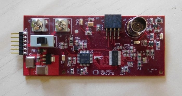
The microcontroller is one of two ICs that provide most of the board’s functionality; the other is a DAC, more specifically, the AD9708 from Analog Devices. This component is a member of the “TxDAC” family of D/A converters. It supports update rates (AKA sample rates) up to 125 million samples per second—more than adequate for my needs.
This particular part has a resolution of 8 bits, though it is pin compatible with 10-bit, 12-bit, and 14-bit versions. This is a handy feature: you can start with the lower-cost 8-bit version, and if you eventually decide that you need more resolution, you can upgrade to one of the higher-resolution (and higher-cost) options without excessively disrupting the existing schematic and layout.

Diagram taken from the datasheet.
As you can see from the application diagram, few external components are needed. A few caps, a resistor for setting the full-scale output current, and (though not shown in the diagram) proper signal-conditioning circuitry for the differential D/A output currents.
Before we move on, I’ll mention some other handy features of this device; keep these issues in mind next time you’re trying to choose the right DAC (which is not a particularly easy task—a Digi-Key search for “DAC” with the “In Stock” option selected gives over three thousand results).
- It’s available as a TSSOP, which is more compact than SOIC (or DIP, of course) but much less troublesome than QFN or any other leadless/microscopic package.
- No external voltage reference is required (though you can use one if you want to).
- Supplying power is easy: a single 3 V or 5 V rail is all you need.
- It accepts parallel input data, which I prefer to serial interfaces. Yes, parallel data requires more pins and takes up more space, but I’m not designing smartwatches, and for me the simplicity of parallel data transfer is a major priority. Just take a look at the “timing diagram”—life may be complicated, but this data interface certainly is not.

Diagram taken from the datasheet.
The Circuit
Here is the DAC portion of my arbitrary waveform generator:

- I have 4.7 µF and 0.1 µF decoupling caps for each power/ground pair.
- DAC_SLEEP is driven directly by a microcontroller GPIO pin.
- The clock signal that controls the D/A circuitry is generated by the microcontroller and applied to the CLK pin.
- The REFLO pin is connected to ground; this enables the internal reference voltage.
- The components/connections for COMP1, COMP2, and REFIO are based on datasheet recommendations.
- Note that COMP1 is connected through a capacitor to the positive supply rail, whereas COMP2 is connected through a capacitor to ground. The COMP1 cap is not essential; the datasheet says that you should include it if you want “optimum performance.” Seriously, though, if your form factor or budget is so restrictive that you have to stress about whether to include a single 0.1 µF ceramic capacitor, you might want to look for a new job.
- The cap on REFIO is required when you’re using the internally generated reference voltage.
- The resistor connected to the FSADJ pin determines the output current when the DAC word is at the maximum value (in this case 255) or at the minimum value (zero, i.e., DB0 to DB7 all logic low). That sounds a bit confusing, I know; it will be clear by the time you finish the article. The FSADJ pin is connected internally to an amplifier circuit that causes the reference voltage to appear at the FSADJ pin. The full-scale current is proportional to the current (called the reference current) flowing out of the FSADJ pin. With a 2 kΩ resistor (and assuming that the internally generated 1.2 V reference is enabled), the reference current is (1.2 V)/(2 kΩ) = 600 µA, which corresponds to a full-scale current of about 20 mA.
The Differential Outputs
The most complicated portion of the DAC design is the output interface. The first thing you need to do is understand what exactly is going on with these IOUTA and IOUTB pins.
The AD9708 has current (as opposed to voltage) outputs. The digital word applied to the data pins directly controls the current flowing out of the IOUT pins, not the voltage that appears at these pins. But why are there two? The datasheet refers to them as differential, but I find this terminology somewhat confusing. When I hear “differential,” I think of signals that use positive and negative polarity, and this makes me think that IOUTA has positive current (i.e., flowing out of the pin) and IOUTB has negative current (i.e., flowing into the pin). But this is not the case. The real situation is conveyed by the following diagram:

So both pins are sourcing current, and in this sense both currents are positive. The “differential” aspect arises from the fact that the current magnitudes are balanced: if one pin has high current, the other has low current. This is why I said earlier that the full-scale current occurs when the input data is at the maximum value or the minimum value. At the maximum value, IOUTA sources the full-scale current; at the minimum value, IOUTB sources the full-scale current. It seems to me that “complementary” would be better than “differential” in this case, but if the experts at Analog Devices prefer “differential,” I’m not going to argue.
Conclusion
Now that we understand the basic DAC hardware connections and the nature of the outputs, the next question is, How do we turn these complementary/differential current magnitudes into a normal voltage signal? Well, that’s kind of a long story, but don’t worry, we’ll cover the details—or at least the details of my implementation—in the next article.
Related Content