Facebook
 Google
 GitHub
 Linkedin
DAC Output Circuitry for an Arbitrary Waveform Generator
How do you convert DAC output currents into a normal voltage signal? Let’s take a look.
How do you convert DAC output currents into a normal voltage signal? Let’s take a look.
I recently designed an arbitrary waveform generator (AWG) board, and I’ve been writing technical articles on the schematic as a way to explore relevant design details before we jump into AWG projects. The two previous articles covered the microcontroller and the DAC, and this article will discuss the signal-conditioning circuitry connected to the DAC’s output pins.
Current to Voltage
The DAC used in the AWG board converts digital data into a somewhat confusing form of analog data. The outputs drive current instead of voltage, and the output signals are complementary (or balanced, or differential—choose your preferred term). If you’ve read the previous article you should have a solid understanding of what exactly these complementary current signals are, but we still have the issue of what to do with them.
We’ll assume that you want to end up with voltage signals instead of current signals. Beyond that, you have options.
- Do you want a single-ended output or a differential output?
- Do you want a signal that is centered around 0 V, i.e., a signal that swings below ground? Or do you want to add a DC offset that keeps the signal above ground?
- Do you have a preference regarding active components vs. passive components?
- Do you want the full performance provided by differential outputs, or would you rather use the DAC as a single-ended device?
Let’s discuss these options before we look at the circuit that I used in the AWG board.
Single-Ended vs. Differential
My guess is that most applications will want a final DAC signal that is single-ended. However, you can prolong the benefits of differential signaling by converting the differential DAC current signals to a buffered differential voltage. This does not require a lot of extra effort from the designer; all you really have to do is use a differential-output amplifier instead of a typical op-amp. The following diagram will point you in the right direction.

Diagram taken from this app note, published by Analog Devices.
AC or DC, Passive or Active?
If you are using the DAC to generate, say, audio signals, you’ll eventually need a waveform that is centered around 0 V. If your signal chain has no need for a waveform that is always above ground, you might as well convert the DAC output directly to an AC-coupled signal. This is easily accomplished using a transformer:
![]()
Diagram taken from the AD9708 datasheet.
I appreciate the simplicity of passive components, but if an active solution is better for your amplification, you can use a dual-supply op-amp circuit that produces a bipolar output signal. An inconvenience with this approach is that you need positive and negative supply voltages. On the other hand, it is advantageous because it is not actually AC-coupled—it produces an output signal that is centered around 0 V, but at the same time it is compatible with low-frequency (or DC) signals. The transformer, in contrast, is strictly for AC applications. The following diagram gives you an example of the bipolar-op-amp approach.

Diagram taken from this app note, published by Analog Devices.
If you want not only DC coupling but also a waveform that remains above ground, you need to configure the op-amp circuit so that it adds an appropriate DC offset to the output signal. This approach is very handy because it works fine when you have only one supply voltage available (and as discussed here, single-supply circuits are very popular these days).

An example of a single-supply output circuit. Diagram taken from the AD9708 datasheet.
Ignoring One of the Outputs
If you are willing to trade performance for simplicity, you can pretend that the DAC is a single-ended device. Ground one of the outputs, then take the current generated by the other output and convert it to a voltage using a typical op-amp current-to-voltage converter (aka a transimpedance amplifier). You can read more about this approach on page 6 of the app note mentioned above.
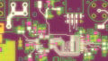
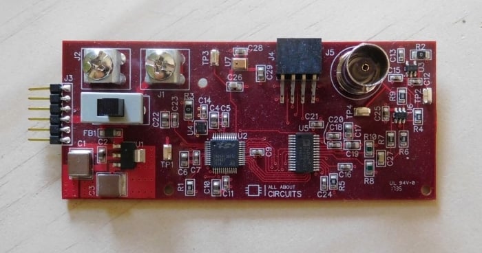
My Circuit
I didn’t want to incorporate a negative power supply into my board, and I didn’t want to use a transformer (I can’t quite remember why...presumably to ensure compatibility with low-frequency and DC signals, or maybe because I’m more familiar with op-amps). I also had no need for a differential voltage signal. Thus, I ended up with the single-supply, single-ended op-amp configuration discussed above. Here’s the circuit:

- The amplifier circuit itself provides a gain of 2; this gain applies to the differential voltage created across R10 and R8. My full-scale output current is ~20 mA, which means that the max voltage swing between the IOUTA node and the IOUTB node is approximately ±0.5 V. If we multiply this by the gain, we find that the max output swing is ±1 V relative to the DC offset.
- The DC offset is 1.65 V (i.e., halfway between ground and the positive supply rail). I prefer to use an integrated circuit instead of a resistive divider when I need a reference voltage. The IC approach offers better performance in terms of precision and noise, and you don’t have to worry about interactions between the resistance in the divider and the rest of the circuit.
- The REF2033 is a handy device because it generates one voltage (VREF) and another voltage that is one-half of VREF (call it VREF/2). This is useful when you need a reference voltage for an ADC and a bias voltage that is used to bias an amplifier at the middle of the ADC’s input range.
- In this case I needed only VREF/2. I was 99% sure that the component would work fine despite the fact that the supply voltage is too low for proper generation of VREF. However, I added R2 and TP2 just to be absolutely sure. These components allow me to disconnect the REF2033 from the 3.3 V rail and manually connect it to the 5 V rail.
- C27 turns the output circuit into a low-pass filter. The capacitance was chosen to create a cutoff frequency of about 1.6 MHz. The formula for the cutoff frequency is shown above in the diagram for the bipolar op-amp circuit.
Conclusion
You can use the link below to download the full schematic. We’ve now discussed the circuitry that forms the functional core of the AWG board. There’s not much to say about the linear regulator, the power-supply switch, etc., and the microphone (U7) is discussed here. In the next article we’ll take a look at the layout.