 Facebook
 Google
 GitHub
 Linkedin
Microcontroller Design for an Arbitrary Waveform Generator
In this article, we’ll look at general concepts and some design details for a circuit board that can output a wide variety of analog signals.
In this article, we’ll look at general concepts and some design details for a circuit board that can output a wide variety of analog signals.
The availability of reasonably priced, high-speed digital-to-analog converters (DACs) opens the door to fairly straightforward circuits that can generate sine waves, triangle waves, ramp waveforms, and so forth. I describe these circuits as “straightforward” because they don’t require sophisticated analog circuitry; the design process is still a bit challenging, but in my opinion the complexity level is fairly low relative to the performance that the circuit provides.
The key concept here is the use of numerical data instead of analog circuits. It would not be easy to design a purely analog board that can produce fully customizable sinusoids, triangle waves, ramps, chirp signals, and modulated radio waveforms. With a digital-to-analog design, we have frequency restrictions and the performance limitations of the DAC, but after that it all comes down to the numbers: one signal path creates many different waveforms because the components are simply converting digital data into an analog signal.
The Board
I recently designed an arbitrary waveform generator (AWG). Here it is:
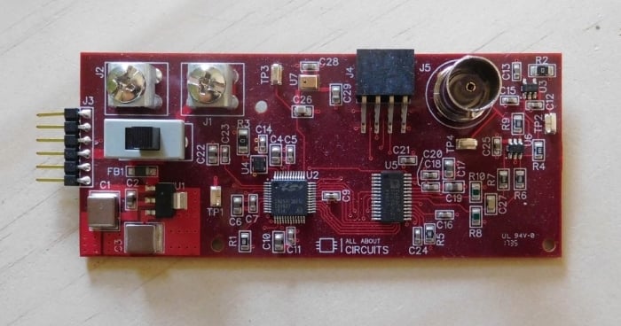
In the near future I’ll incorporate this board into some projects. Before that, though, we’ll discuss the technical details via separate articles. After all, it’s a good idea to know how and why something works before you start using it. As you can probably see in the photo, the design consists of two main integrated circuits and numerous smaller support components. The two main ICs are a high-speed microcontroller and a high-speed DAC. In this article we’ll focus on the microcontroller.
The MCU
I limit myself to Silicon Labs microcontrollers, because they are excellent devices and (maybe more importantly) because I am thoroughly familiar with them. Even with this restriction, though, there are many to choose from. I decided on the C8051F360, and in this case the decision was easy: I wanted the highest possible clock speed, which for SiLabs MCUs is 100 MHz. Only two of their 8051 families support a core frequency of 100 MHz, and one of those families is not compatible with the new SiLabs IDE. So I was left with the C8051F36x family, and among these parts the C8051F360 is the most capable in terms of pin count and peripherals.
Power
First things first: the decoupling capacitors. I have 0.1 µF caps for each power/ground pair and 4.7 µF caps for three of the four pairs.

This is a generous decoupling scheme, and I decided to eliminate one of the 4.7 µF caps when I realized that it was clogging up a challenging portion of the layout.
I/O Connections
The next schematic excerpt conveys the MCU’s primary digital and analog input/output connections.

The design uses only two digital peripherals: a UART module and an output from the programmable counter array (PCA). The UART signals go to a USB-to-UART adapter board, which enables convenient serial-port-style communication between the MCU and a PC.
The PCA output is used as the clock that drives the DAC, and it also causes the MCU to output the next byte of DAC data. Why do I have the DAC_CLK signal connected to two I/O pins? This is just one of the “backup plans” that I regularly incorporate into my PCBs. I had minor doubts about the interrupt scheme I was planning to use, and I always have vague fears about making some sort of mistake with crossbar pin assignments. In this case I was probably being excessively cautious, but the bottom line is that if I’m not 100% sure about something, I try to incorporate a workaround. It is so much easier to solve problems before the PCB has been fabricated and assembled.
Here are descriptions of the other connections:
- The internal reference voltage (used for analog-to-digital conversion) is output on P0.3. The values of the two bypass capacitors are based on datasheet recommendations (see page 67).
- The clock signal (generated by a MEMS silicon oscillator) enters the MCU through the XTAL2 pin. I could have used the MCU’s internal oscillator, but since this is theoretically a timing-sensitive application, it was more appropriate to use a high-precision external oscillator.
- DAC_SLEEP can be used to put the DAC in a low-power state.
- MIC_OUT is the output signal from a MEMS microphone; it connects to P1.6, which can be routed to the microcontroller’s ADC.
- The 8-bit DAC data is driven on P2. I made sure to dedicate an entire 8-bit port to these signals so that I could drive new DAC data using just one statement, e.g., “P2 = 0xAA” or “P2 = DAC_data[n]”; we’re trying to maximize speed here, and each additional processor instruction limits the rate at which we can update the DAC output.
Programming and Debug
The programming/debug pins (C2CK and C2D) are connected to the appropriate pins on connector J4, which mates with the corresponding connector on my C2 adapter board. I also have GPIO pins connected to J4 so that I can use the test/debug components on the adapter board.


The C2CK pin is also the reset pin. There is a ~100 kΩ internal pull-up resistor on the reset line, so an external pull-up isn’t strictly necessary. However, an external 1 kΩ pull-up provides extra protection against spurious resets by establishing a lower-impedance path to the supply rail.
Conclusion
We discussed the general idea of a DAC-based arbitrary waveform generator, and we took a detailed look at the microcontroller portion of the schematic. In the next article we’ll cover the digital-to-analog converter.
Related Content


what is the bandwidth and is there any firmware you shared or would like to share
It will be interesting if you discuss about MCU clock frequency and actual rate of DAC output change as in a MCU each instruction take normally more than one clock tick to complete. For high speed DAC to be controlled at full speed, perhaps the MCU clock frequency must be a number of times the DAC speed.