 Facebook
 Google
 GitHub
 Linkedin
Design a Custom Microcontroller Programming and Testing Board
In this article we’ll discuss the design for a custom microcontroller programming/debug/extension PCB and we’ll look at an example project.
In this article we’ll discuss the design for a custom microcontroller programming/debug/extension PCB and we’ll look at an example project.
Related Information
- The EFM8 Series from Silicon Laboratories: A Powerful New Embedded Development Platform
- Custom Microcontroller Design: Assembling, Measuring, Programming
- Custom Microcontroller Design: Hardware, Tools, and Toolchain
Custom MCU Boards
One thing that I find consistently tiresome with custom microcontroller designs is the need for programming and basic testing hardware.
Programming/Debug
Obviously you need a way to load program code into your microcontroller, and thus you have to include hardware that allows you to connect the relevant pins on the MCU to the programmer module. The most convenient approach is a connector that mates directly to the programmer cable, but you could also use a different connector in conjunction with some sort of cable assembly.
This programmer connection can also be referred to as the debug connection, because the same signals can be used for debug execution through the integrated development environment (IDE). However, it’s important to remember that programming is by far the more important functionality. It is theoretically possible to develop microcontroller applications without the use of breakpoints and register inspection and what not, but you will certainly get nowhere fast if you have no way to download code into the device.
Basic Testing
An enduring problem with electrons is that they are invisible. The result is that a perfectly functional microcontroller looks the same as a nonfunctional one (or an empty IC package, for that matter). This is why your board needs circuitry that allows you to confirm that the MCU is actually powered and properly executing code. The classic solution here is an LED or two; this type of visual feedback is limited but adequate in many cases.
The Problem
What annoys me about all this is that programming and testing hardware is not needed by the final application and yet it consumes design time and board space.
I don’t get paid by the hour to design PCBs, so it’s irksome to incorporate LEDs, resistors, connectors, etc. into every single schematic and PCB that I create. Copy and paste can save some time, it’s true, but copying and pasting is not so easy with the layout, and of course everything has to be double-checked or otherwise diligently handled so as to ensure that there are no unpleasant surprises when the board comes back from the assembly house.
As far as board space, I think you all know that large circuit boards have gone out of fashion. Designers need to be in the habit of reducing or even minimizing component area, and in this age of microscopic integrated circuits a couple LEDs and their associated resistors can be a non-trivial contribution to the size of the PCB. A large connector for direct mating to the programmer module is far worse, and the situation deteriorates rapidly if you want to incorporate additional forms of feedback, such as an LCD or a buzzer.
The Solution
To me it makes a lot of sense to offload this functionality onto a separate PCB that is used just for programming and development. For example:

Here are the advantages:
- The only additional component on the application board is the connector that brings the relevant signals to or from the adapter board (or programmer board, or debug extension board, or whatever you want to call it). A typical 0.1-inch connector is convenient, but you could certainly use something more compact if you’re so inclined.
- You can incorporate all sorts of test/debug functionality without any significant increase in the complexity or size of the application board.
- If you manage to get a fully functional adapter board back from the assembly guys, you’re set. No more worrying, no more double-checking. All you have to do is ensure that the application board has the right signals going to the right pins and you know that you’ll have a working programming/debug interface—or if it doesn’t work, you know that the problem is somewhere on the application board, not in the programming/debug hardware.
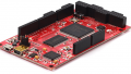
My Adapter Board
I prefer Silicon Labs microcontrollers, so I designed a C2 adapter board. “C2” is SiLabs’s name for their two-wire (plus ground) programming/debug interface designed especially for low-pin-count MCUs. Here’s the schematic:

Some comments:
- I prefer to have non-visual feedback; this is helpful if you want to test the board when it’s inside an enclosure or in any other situation that prevents you from easily seeing the PCB. Thus, I added a buzzer (BZ1).
- BZ1 is a magnetic transducer, and that means you need a flyback diode. Hence D1. Why did I use a two-diode component when I only need one diode? Because I live in perpetual fear of diodes being inserted with the wrong polarity, and my goal with every PCB is to open my mailbox and find a fully functional PCB that requires zero rework. I especially despise surface-mount rework. The dual-diode component comes in a three-pin package that cannot be assembled incorrectly. (I chose three-pin LED packages for the same reason.) It’s also a more versatile component; if a future board needs two diodes, I already have the component in my library and ready for action.
- The connector coming from the SiLabs debug adapter provides a 5V supply that can source up to 100 mA. I use this supply to drive the buzzer.
- J3 is an extension option, i.e., a second application board could be connected as a way to extend the functionality of the first application board.
If you are using Silicon Labs microcontrollers that support the C2 interface, you can simply duplicate my design and you’ll have a handy programming/debug/testing board. If you prefer MCUs from other manufacturers, you can use this schematic as a guide and make modifications as necessary.
Here's the BOM:
|
Reference Designator |
Description |
Manufacturer p/n |
|
BZ1 |
buzzer |
CT-1205-SMT-TR |
|
C1 |
ceramic capacitor, 4.7 µF |
EMK212B7475KG-T |
|
C2 |
ceramic capacitor, 0.1 µF |
GRM188R71C104KA01D |
|
D3 |
diode array, general purpose |
BAV23CLT1G |
|
J1 |
header, 10-pin, male |
3020-10-0300-00 |
|
J2 |
header, 8-pin, male |
610108249121 |
|
J3 |
header, 8-pin, female |
610108249221 |
|
LED1 |
green LED |
AM23SGC-F |
|
LED2 |
red LED |
AM23ID-F |
|
Q1 |
NPN transistor |
DSS20201L-7 |
|
R1 |
resistor, 100Ω, 1/8W |
RC0805FR-07100RL |
|
R2 |
resistor, 100Ω, 1/8W |
RC0805FR-07100RL |
|
R3 |
resistor, 360Ω, 1/8W |
RC0805FR-07360RL |
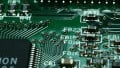
Let’s take a quick look at the PCB layout:

- I used surface-mount components for everything, including the connectors. I have a vague idea that this can reduce assembly costs because it eliminates extra steps associated with through-hole components, and it can also facilitate routing on the bottom side.
- J2 is the primary application-board connector. I chose a male connector here so that the exposed pins would be on the adapter board instead of the application board.
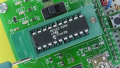
- J1 is keyed (see photo below). It is so helpful to have a connector that prevents incorrect mating.

An Example Project
In the following photo you see the adapter board connected to an application board that will appear in future projects.

The adapter board was used to load a simple program into the EFM8 Laser Bee microcontroller on the application board. The program uses both LEDs and drives the buzzer with frequencies chosen to produce standard musical notes. The square wave that drives the buzzer is generated via the Programmable Counter Array; the frequency is controlled by writing an appropriate divider value into the PCA0CPH2 register. The PCA itself is driven by a ~255 kHz clock, and the following code shows the PCA0CPH2 values corresponding to the different notes:
//musical notes
#define NOTE_C6	122	//1046.50 Hz
#define NOTE_D6	109	//1174.66 Hz
#define NOTE_E6	97	//1318.51 Hz
#define NOTE_F6	91	//1396.91 Hz
#define NOTE_G6	81	//1567.98 Hz
#define NOTE_A6	73	//1760.00 Hz
#define NOTE_B6	65	//1975.53 Hz
#define NOTE_C7	61	//2093.00 Hz
#define NOTE_D7	54	//2349.32 Hz
#define NOTE_E7	48	//2637.02 Hz
The code simulates a concert that begins with Beethoven’s 5th. The green LED flashes according to the notes. The orchestra first warms up with a C major scale, then the red light turns on to shush the audience, then the performance begins. Here’s a video:
The code is not particularly complicated. One little detail is that the PCA is briefly disabled to create audible separation between notes, as follows:
PCA0CN0_CR = 0;	//disable the PCA to silence the buzzer
Delay_10ms(2);
PCA0CN0_CR = 1;	//re-enable the PCA
C2ADAPTER_LEDGRN = HIGH;
Delay_10ms(5);
C2ADAPTER_LEDGRN = LOW;
Delay_10ms(43);
If you want more details, feel free to download all of the source and project files by clicking on the following link:
Conclusion
In this article we looked at a microcontroller adapter board that can reduce the size and complexity of your microcontroller-based PCBs. It also makes the initial testing phase more straightforward. We finished with a simple project that uses the adapter board’s LEDs and magnetic buzzer.
Give this project a try for yourself! Get the BOM.


Is this open source, cause i think i can use this board design for my ESP-01 module and link it to my Arduino and make a couple of non-breadboard designs in a smaller space. Awesome layout though. Great pinouts. Question, if i pinouts a larger chipset, any thought as to what resistors to use with a 3.3 to 5V switchoff? Any help welcome. But thank you in advance.