Facebook
 Google
 GitHub
 Linkedin
Negative Feedback, Part 8: Analyzing Transimpedance Amplifier Stability
The techniques discussed in previous articles can help us to understand and remedy stability problems observed in a common circuit used to amplify photodiode signals.
The techniques discussed in previous articles can help us to understand and remedy stability problems observed in a common circuit used to amplify photodiode signals.
Previous Articles in This Series
- Negative Feedback, Part 1: General Structure and Essential Concepts
- Negative Feedback, Part 2: Improving Gain Sensitivity and Bandwidth
- 316207Negative Feedback, Part 3: Improving Noise, Linearity, and Impedance324
- Negative Feedback, Part 4: Introduction to Stability325
- Negative Feedback, Part 5: Gain Margin and Phase Margin326
- Negative Feedback, Part 6: New and Improved Stability Analysis
- Negative Feedback, Part 7: Frequency-Dependent Feedback327
Supporting Information
- Introduction to Operational Amplifiers
- Operational Amplifiers: Negative Feedback329
- AC Phase
- Practical Analog Semiconductor Circuits331Special-Purpose Diodes
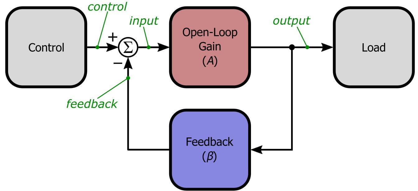
Just so you don’t have to switch pages if you want to ponder the general feedback structure, here is the diagram presented in the first article:
Even Internally Compensated Op-Amps Can Oscillate
Not many engineers these days are incorporating flagrantly unstable discrete BJT amplifiers into their designs. This makes life less exciting, though somewhat more stable, because most op-amps are internally compensated to the point that they have adequate phase margin even with closed-loop gain of unity (i.e., β = 1). Internal compensation is certainly convenient, especially for engineers who don’t have much experience with stability issues. But it also encourages a problematic complacency—problematic because even an internally compensated op-amp can oscillate, and if it does, the forlorn designer may not understand whence this instability has come or how to properly redress it.
Before we move on to our simulations, let’s take a look at internal compensation in view of our ever-increasing expertise with stability analysis. Consider this open-loop gain plot for the LT1001 op-amp from Linear Tech.
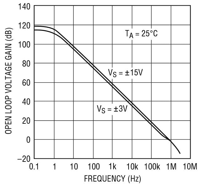
One way to think of internal compensation is in terms of the dominant low-frequency pole that causes the open-loop gain to reach unity when the phase shift is still far from 180°. But this plot reminds us that we can view internal compensation in a different way: the dominant low-frequency pole ensures that the slope of the open-loop roll-off is 20 dB/decade all the way to unity gain. Recall the alternative approach to stability analysis: if the difference between the slope of the loop gain’s magnitude response and the slope of the feedback network’s magnitude response is not greater than 20 dB/decade at the point of intersection, the amplifier is sufficiently stable. The inevitable higher-frequency poles—you can just discern an increase in the roll-off slope at about 3 MHz—do not endanger stability because β would have to be greater than 1 to make the 20log(1/β) and 20log(A) curves intersect at a point that falls within the -40 dB/decade segment of the open-loop magnitude response.
However, as we learned in the previous article, it is quite easy to create instability even when the slope of the amplifier’s open-loop roll-off does not exceed 20 dB/decade—all you need is some frequency response in the feedback network.
Beware Hidden Capacitance
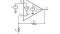
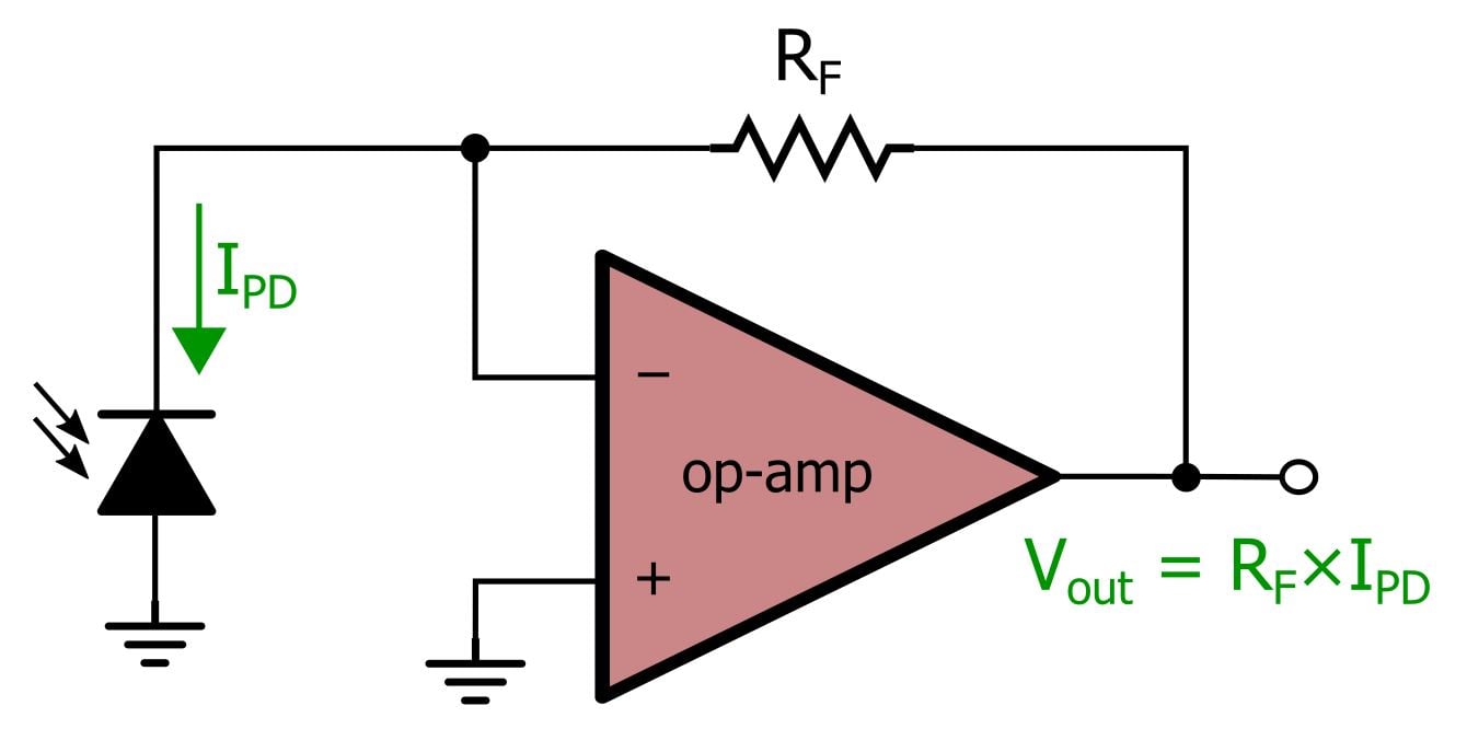
A photodiode configured for “photovoltaic mode” (meaning zero-volt bias across the photodiode, as opposed to “photoconductive mode” in which the photodiode is reverse-biased) functions essentially as a light-dependent (or UV-dependent, or IR-dependent) current source. The small currents generated by the diode are amplified and converted into a voltage by a transimpedance amplifier (TIA), as follows:
Everything looks fine: internally compensated op-amp, non-frequency-dependent feedback network . . . but there is trouble lurking inside that seemingly innocuous photodiode. This is what the TIA looks like if we replace the photodiode with an equivalent circuit:
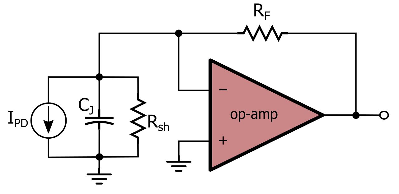
The diode’s shunt resistance could theoretically influence the DC gain, but much more importantly, the junction capacitance has introduced frequency response into the feedback network.
Simulate!
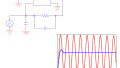
Here is the first LTSpice schematic that we will use to analyze the stability of a typical photodiode TIA.
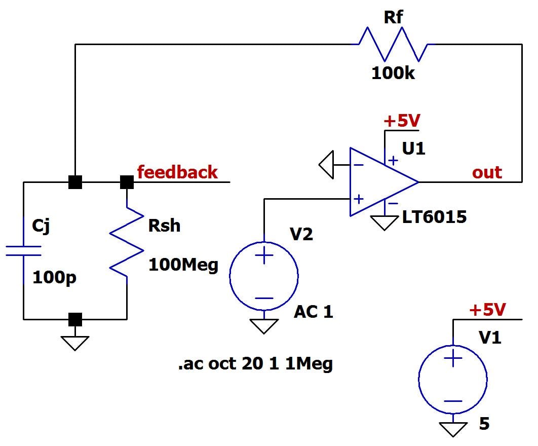
This circuit incorporates reasonable values for the junction capacitance, shunt resistance, and feedback resistor. Just as in the previous article, we have separated the feedback network from the op-amp, because this allows us to generate open-loop gain plots by grounding the negative input while applying an AC source to the positive input. The voltage that would be fed back and subtracted is labeled “feedback,” such that we can obtain a 20log(1/β) curve by plotting 20log(1/(Vfeedback/Vout)).
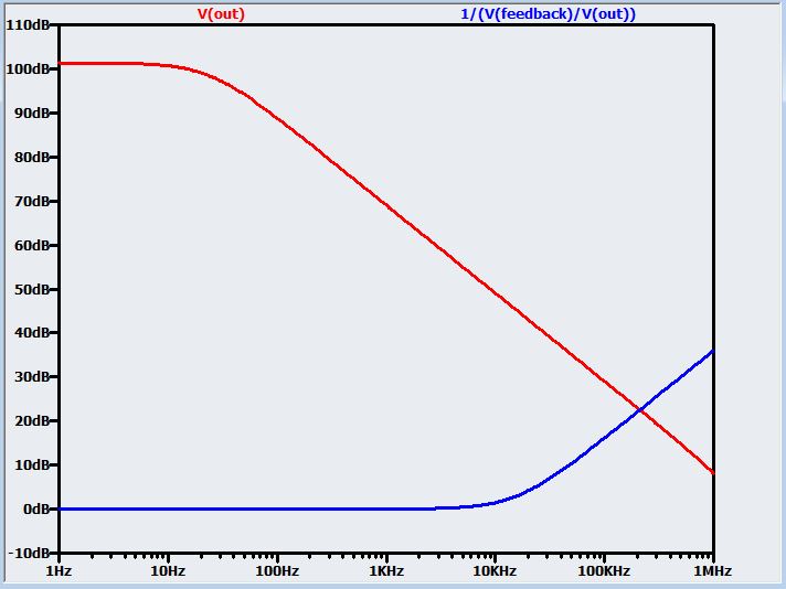
The problem is immediately apparent: the diode’s junction capacitance introduces a pole into the feedback network (remember from the previous article that a pole in the β transfer function looks like a zero when we plot the frequency response of 1/β). You can intuitively understand this by thinking about how low- and high-frequency signals pass through the feedback circuit: The capacitor is an open circuit at DC. The shunt resistance can also be approximated as an open circuit because it is so much larger than the feedback resistor. So at low frequencies, Vfeedback ≈ Vout, and thus β ≈ 1. As frequency increases, Rsh is still approximately an open circuit, but the impedance of Cj gradually decreases. This leads to gradually decreasing β, which translates into a positive slope in the amplitude of the 20log(1/β) curve. Consequently, at the point of intersection, the slope of 20log(A) is -20 dB/decade and the slope of 20log(1/β) is +20 dB/decade; the difference in slopes is 40 dB/decade, so the circuit is not sufficiently stable.
Compensate!
We can’t do much to change the feedback pole itself, because its location is determined by the resistor that sets the closed-loop gain and the properties of the photodiode—presumably these aspects of the circuit are governed by non-negotiable system requirements. Thus, we need to compensate for this pole, and we do that by introducing a zero into the feedback network. As we saw in the previous article, a capacitor in parallel with the “lower” feedback resistor (in this case Rsh) creates a feedback pole, and a capacitor in parallel with the “upper” feedback resistor (in this case RF) creates a feedback zero. So we need capacitance in parallel with RF, as follows:
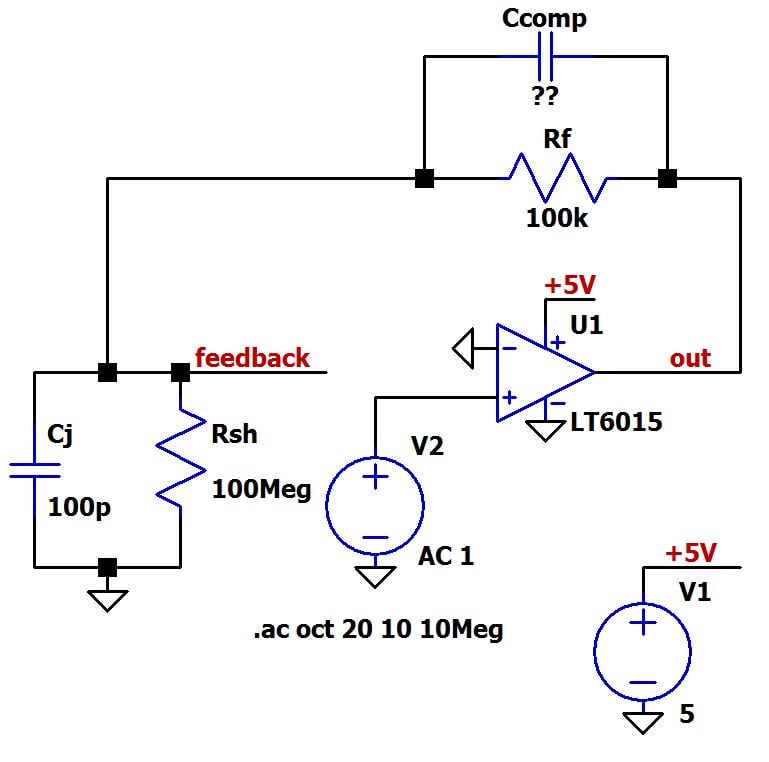
The question is, how much capacitance? The general procedure is to start with an approximate value and then use adjust-and-check simulations to find the sweet spot. If you have experience with photodiode TIA circuits, you probably have a general idea of how much compensation capacitance is needed. Otherwise, find the intersection frequency (fint) from the simulated plot of 20log(A) and 20log(1/β) and then use the following formula:
\[C_{comp}=\frac{1}{2\pi R_FF_{int}}\]
This will not give you consistently accurate results because it does not take the junction capacitance into account, but the result should be close enough to serve as a starting point for adjust-and-check simulations. In our circuit, we have the following:
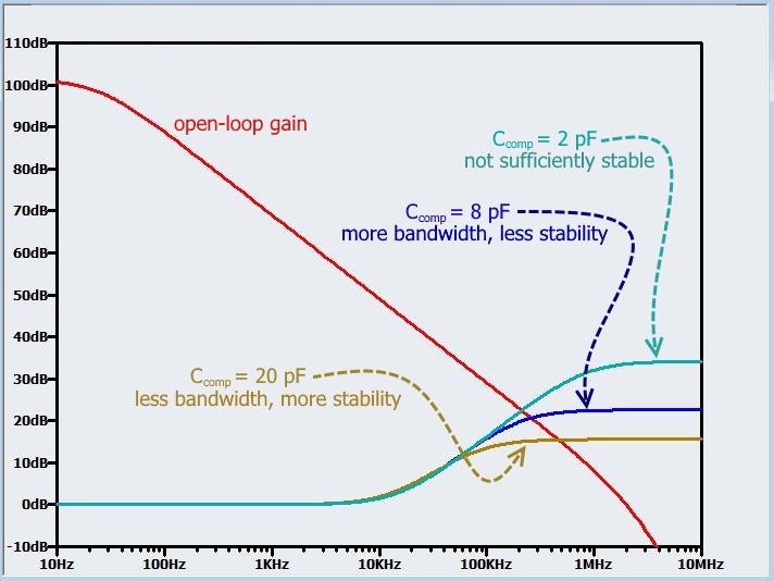
\[C_{comp}=\frac{1}{2\pi\left(100\ k\Omega\right)\left(210\ kHz\right)}\approx8\ pF\]
Before we complete this compensation procedure, we need to decide where exactly we want the feedback zero to be. To achieve sufficient stability, the 20log(1/β) curve must have slope ≈ 0 when it intersects the 20log(A) curve, so we know that the zero frequency cannot be higher than the intersection frequency. Next we have a trade-off: If the zero is very close to the intersection frequency, the circuit will have lower (though probably adequate) phase margin and maximum closed-loop bandwidth. As the zero frequency decreases from this point, phase margin increases but closed-loop bandwidth decreases. You can think about the trade-off as follows:
- Locate the zero well below the intersection frequency:
- if you do not expect high-frequency photodiode signals
- if you want to filter out high-frequency components in the photodiode signals
- if your circuit is likely to be exposed to operational or environmental conditions that could significantly affect the frequency response of the amplifier or the feedback network
- Locate the zero very close to the intersection point:
- if you need to maximize the TIA’s usable bandwidth
This plots shows the stability results for three different Ccomp values:
Conclusion
This photodiode TIA circuit has provided an excellent opportunity for applying the alternative stability-analysis method to frequency-dependent feedback. The next article will introduce an additional stability-analysis simulation technique and demonstrate the use of this technique in the context of another situation that can degrade the stability of an internally compensated op-amp.
Next Article in Series: Negative Feedback, Part 9: Breaking the Loop
Related Content