 Facebook
 Google
 GitHub
 Linkedin
Negative Feedback, Part 10: Stability in the Time Domain
The transient response of a negative-feedback amplifier can help us to understand the nature of stability and convey useful information about the stability characteristics of a particular circuit.
The transient response of a negative-feedback amplifier can help us to understand the nature of stability and convey useful information about the stability characteristics of a particular circuit.
Previous Articles in This Series
- Negative Feedback, Part 1: General Structure and Essential Concepts
- Negative Feedback, Part 2: Improving Gain Sensitivity and Bandwidth
- Negative Feedback, Part 3: Improving Noise, Linearity, and Impedance
- Negative Feedback, Part 4: Introduction to Stability
- Negative Feedback, Part 5: Gain Margin and Phase Margin
- Negative Feedback, Part 6: New and Improved Stability Analysis
- Negative Feedback, Part 7: Frequency-Dependent Feedback
- Negative Feedback, Part 8: Analyzing Transimpedance Amplifier Stability
- Negative Feedback, Part 9: Breaking the Loop
Supporting Information
Time vs. Frequency
There is no doubt that comprehensive, accurate stability analysis must take place in the frequency domain. Loop gain, phase shift curves, pole locations, roll-off slope . . . all the analytical tools that we use to assess stability are inextricably linked to the general technique whereby we evaluate a circuit’s behavior as a function of signal frequency. However, the frequency domain is, in a certain sense, less “real” than the time domain. The purely physical realm of human life is governed by three dimensions of space and the rather mysterious phenomenon we call time. Consequently, our most direct interaction with a circuit occurs when we observe voltages or currents in relation to time rather than the frequency of a theoretical sinusoidal signal passing through that circuit.
With this in mind, we can readily see the value of pondering the ways in which the transient response of a negative-feedback amplifier can 1) strengthen our intuitive understanding of stability and 2) help us to make an initial assessment of stability characteristics without recourse to frequency-domain analysis. As usual, we will employ simulations to elucidate the concepts being discussed. You could by all means apply these concepts to oscilloscope measurements with real circuits, but you have to keep in mind that such measurements involve a variety of error sources—sampling artifacts (for digital scopes), parasitic capacitance and inductance, the scope’s input impedance, and grounding issues come to mind. For example, in the previous article we saw that a mere 30 pF of load capacitance could lead to nontrivial reduction in the phase margin of an op-amp circuit. If your scope’s input stage contributes 15 pF and you have another 10 pF from the probe, your circuit may appear more unstable than it actually is.
Back to the BJT Amp
The simple (and highly unstable!) BJT amplifier that we introduced in Part 5 will provide fast, accurate transient simulations. Here is the circuit diagram:
Note that the feedback node is now connected to the base of Q2. Before, we grounded the base of Q2 because we were measuring the open-loop gain (separated from the feedback network), and then we plotted Aβ mathematically—i.e., we told LTSpice to multiply the open-loop response by the feedback factor and plot the result.
The Step Response
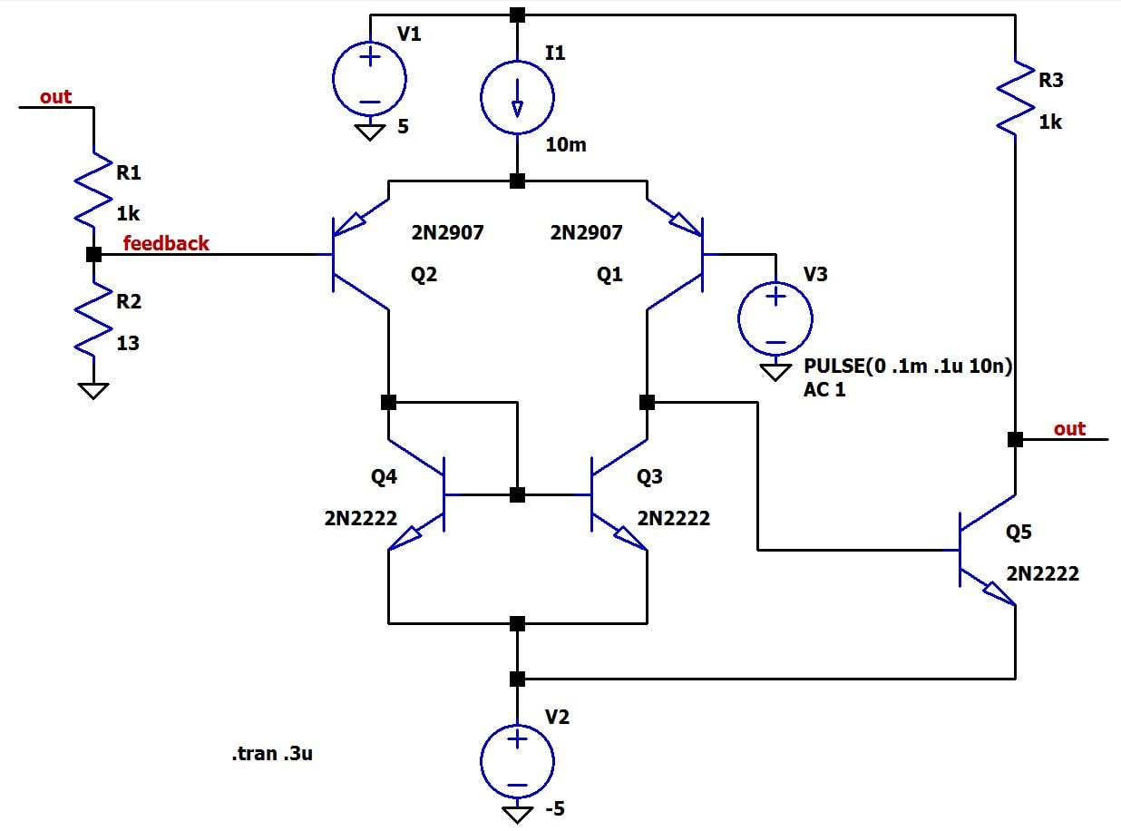
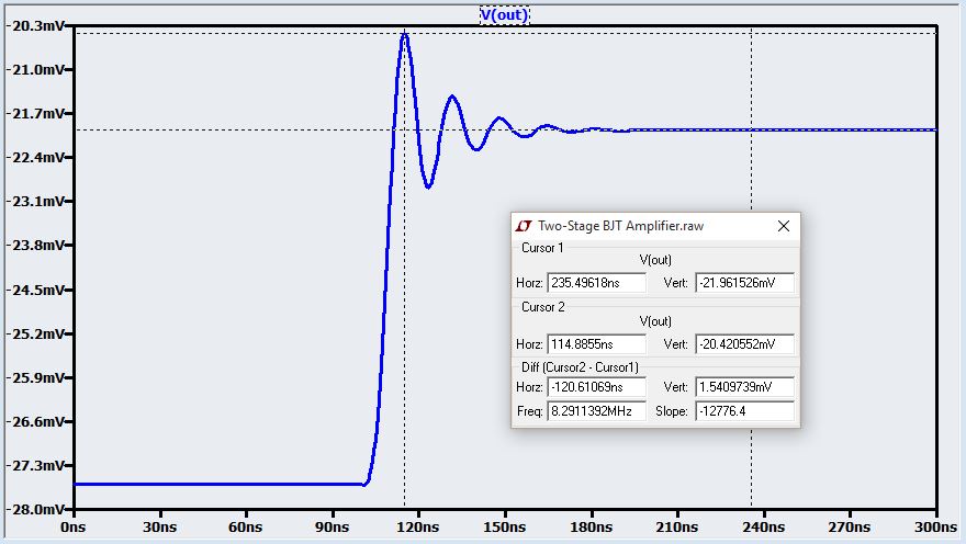
Our goal with these transient simulations is to flood the amplifier with a variety of high-frequency signals so we can see if any of them will coax the circuit into oscillation. This is actually much simpler than it sounds: all we need is a rapid change from one steady voltage to another. The Fourier transform of a step function tells us that a pulse with a rapid rising edge will contain at least a small amount of energy up to very high frequencies. Thus, applying an approximation of a step function allows us to stir up any oscillations to which the circuit might be susceptible. In these simulations we use a 100 µV input step with a rise time of 10 ns. Let’s take a look at the step response for the feedback network shown above, which corresponds to β = 0.013 and phase margin = 45°.
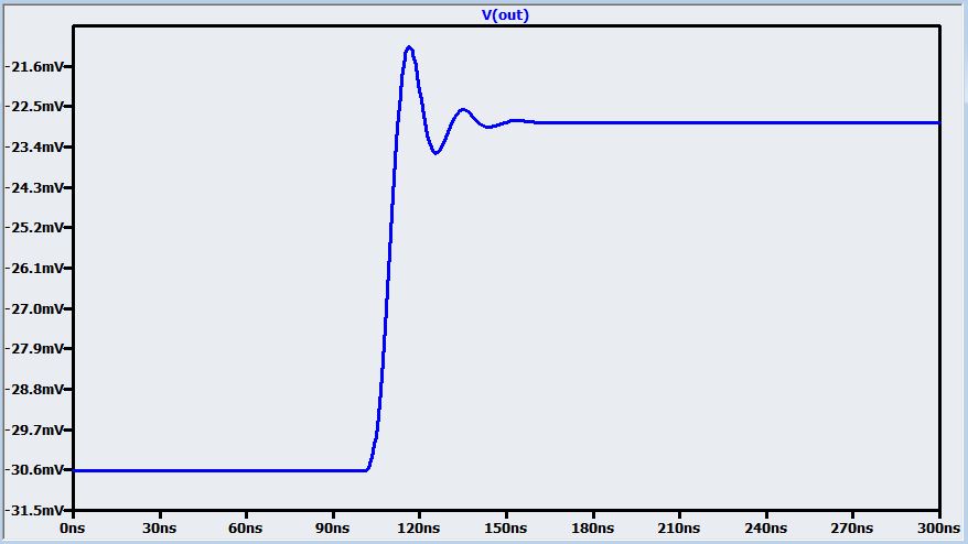
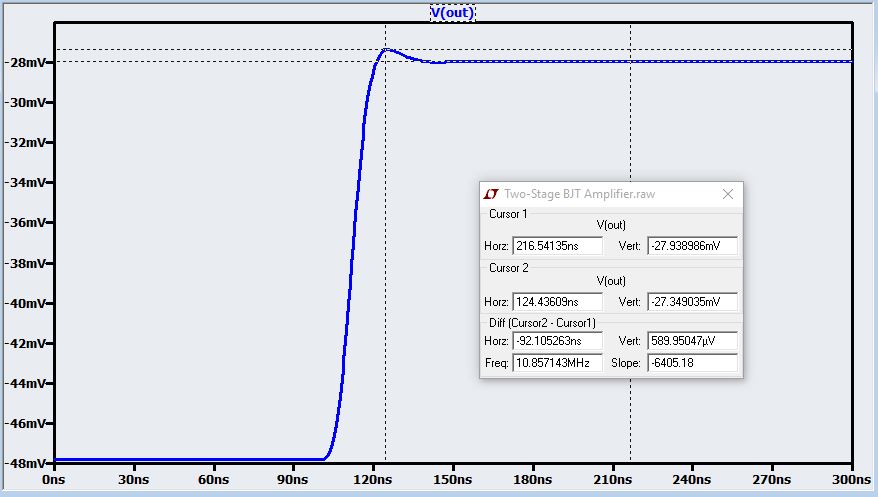
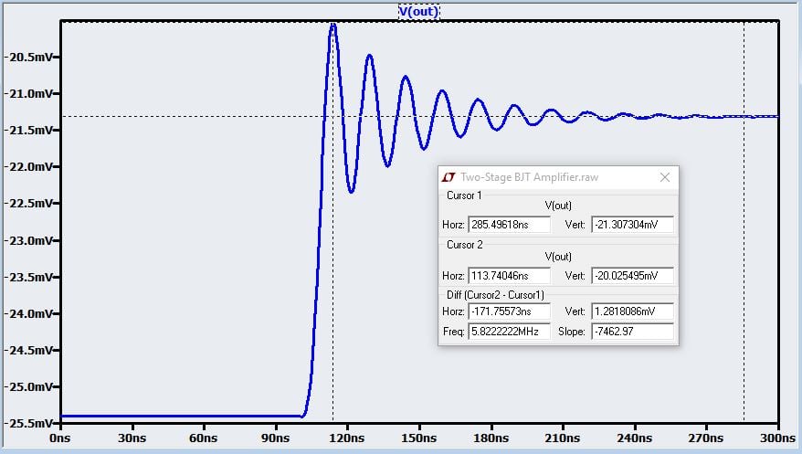
The first thing to notice is that this sufficiently stable amplifier is by no means free of overshoot. A phase margin of 45° does not mean that the step response will perfectly reproduce the input signal. Actually, there is always a compromise between response time and overshoot—this is simply the nature of negative feedback. If you make β small enough to eliminate all overshoot, you end up with a system that takes too long to settle on the final value, as demonstrated in the following plot:

In the middle plot we see some overshoot even when β is far below the value that gives us a sufficiently stable amplifier. In the bottom plot we have eliminated overshoot, but instead we have a sluggish step response that takes three or four times as long to reach the appropriate output level.
From Overshoot to Phase Margin
It is possible to derive a mathematical relationship between phase margin and overshoot percentage, where the latter is calculated as (Vpeak – Vfinal)/(Vfinal – Vinitial). This is a very useful thing, because it allows us to determine a circuit’s approximate degree of stability with nothing more than the measured or simulated step response. The following plots show our BJT amplifier’s step response as β increases. The caption beneath each plot indicates the phase margin (obtained from separate frequency-domain simulations), the theoretical overshoot percentage for this phase margin, and the measured overshoot percentage. (Page 17 of this app note from Texas Instruments has a graph that you can use to find the expected overshoot for a particular phase margin, or vice versa.)
phase margin: 70°; theoretical overshoot: ~2.5%; measured overshoot: 3%
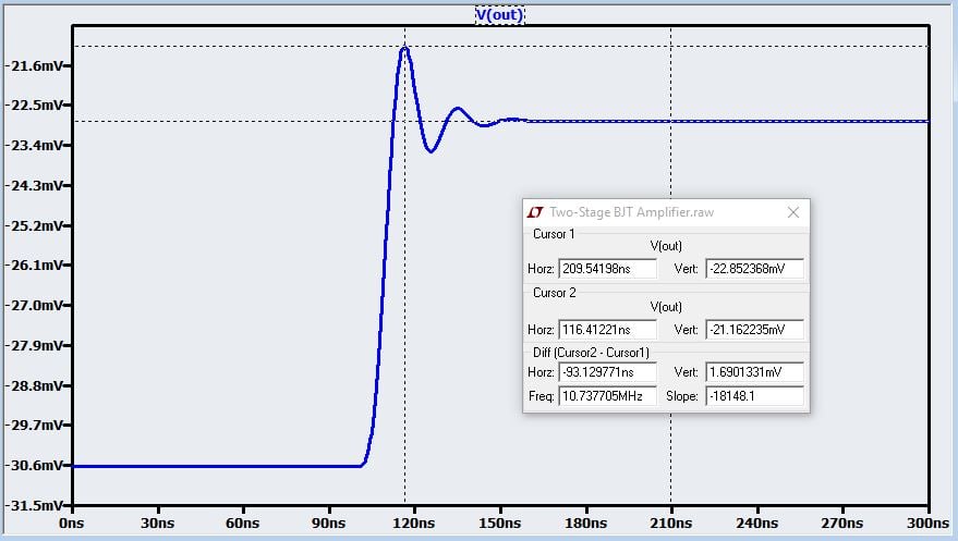
phase margin: 45°; theoretical overshoot: ~23%; measured overshoot: 22%
phase margin: 35°; theoretical overshoot: ~33%; measured overshoot: 27%
phase margin: 25°; theoretical overshoot: ~47%; measured overshoot: 31%
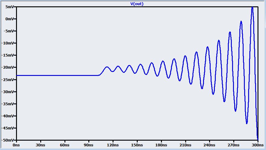
β too high; amplifier not stable
We can see that the measured results are consistent with theoretical results for higher phase margins. Agreement between theory and simulation appears to deteriorate as the phase margin decreases, perhaps because the transient response is affected by some sort of nonlinearity as the circuit approaches instability. But this does not significantly diminish the value of analyzing step response, because the lower phase margins are not particularly relevant for practical design purposes—almost any negative-feedback amplifier needs to have phase margin greater than 35°.
Visualizing Loop Gain
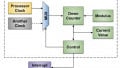
You may recall the following diagram from a previous article:
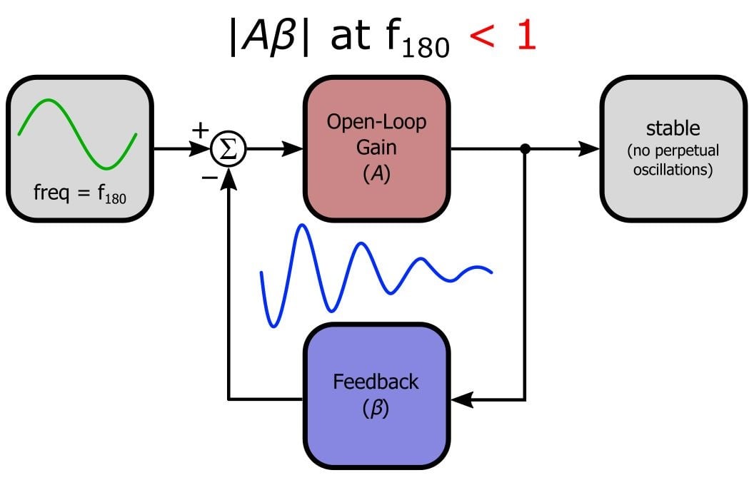
Now look back at the transient waveforms presented in the preceding section. The similarity is illustrative: In the diagram, the damped sine wave represents the way in which the loop gain attenuates oscillations that are created by phase shifted signals reinforcing each other. Even though phase shift of 180° occurs at a certain frequency, stability is maintained because the loop gain is less than unity at this frequency. These signals experience positive feedback, but their amplitude nonetheless decreases over time—the loop gain does not allow them to increase. We see a very similar attenuating effect in the transient response. The high-frequency energy in the step signal stirs up oscillations, but as long as the loop gain fulfills the stability criterion, the amplifier keeps the oscillations under control. Higher phase margin indicates lower loop gain at the frequency corresponding to 180° phase shift, so the circuits with higher phase margin suppress these oscillations more quickly.
Conclusion
We have covered quite a wide variety of topics related to the theory and practical implementation of negative feedback in the context of amplifier circuits. We began with the general negative-feedback structure and then discussed the benefits to be gained by incorporating negative feedback into an amplifier design. We then moved to an in-depth exploration of frequency-domain stability analysis, and now we have concluded this series by demonstrating the relationship between stability and transient response. If you are still unsure about anything, or if your life seems a little unstable, just go back to Part 1 and keep reading until everything is crystal clear.
Related Content


First rate presentation of the theory of negative feedback. This should be the basis, along with lab experiments, of course curricula for second year university electrical engineering. Hats off!
I ran into both of these issues when designing a 4-terminal I-V converter for solar cell quantum efficiency measurements. Incorporating bias, and trapezoidal generation of current (chopper), and having currents to 25 mA made things more interesting. Everything worked dandy until the calibration cell, which was larger, and thus had more capacitance was connected.
I was not given enough time to solve the offset problem which was about 40 pA DC. It was insignificant anyway. I had no manual method to alter the offsets. I had planned to do it electronically using two gains and the I-V converter reconfigured to voltage mode, BUT my offset D/A could not output exactly zero volts.
The lock-in only cared about AC performance and +-40 pA in the operating point made no difference.
I also incorporated an Open circuit voltage mode, A 2 terminal/4 Terminal mode and a +-50 mA suppress mode The zero check and zero correct modes didn’t work. The output included peak detectors and a bi-color LED. The output was +-10 Volts, so you got lots of dynamic range if you used one scale.
Biasing was +-10 V without suppression and +-5V with suppression. The usual operating points were 0 to -1.5 V.
Aside: For photodiodes there are two different modes of operation: Photovoltaic and photoconductive.
The OP amps require careful selection with Vos and Ib being the most important.
I love that pun at the end stating, “if your life seems a little unstable, just go back to Part 1 and keep reading until everything is crystal clear.” Starting with part 8, I went to digest every part from 1 to 10. Thank you so much for the help!