Facebook
 Google
 GitHub
 Linkedin
Rambus Introduces PCIe 7.0 Switch With Time-Division Multiplexing
The new switch IP targets AI and data center SoCs that need to move data efficiently across CPUs, GPUs, accelerators, and NVMe storage without adding more physical lanes.
Rambus has introduced a PCIe 7.0 Switch IP with time-division multiplexing (TDM), designed to help system architects build scalable AI and high-performance computing (HPC) fabrics without the complexity of simply adding more PCIe lanes and endpoints.
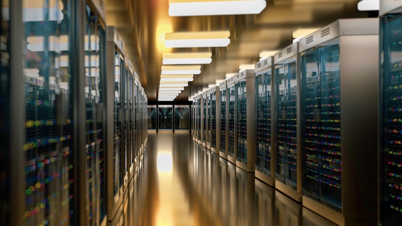
The next wave of AI and data center SoCs will need high bandwidth density, advanced traffic management, and large scalability. Image used under Adobe Stock license
The San Jose-based IP company announced the addition earlier this month, positioning it as a way to improve link utilization across shared connections in data centers where AI training, inference, and large-scale data movement compete for the same interconnect bandwidth.
The switch IP is built on the PCIe 7.0 specification and slots into Rambus's existing portfolio of PCIe 7.0 controllers, retimers, and debug solutions. Together, the product line provides SoC designers with a comprehensive set of PCIe 7.0 building blocks for next-gen AI infrastructure.
What TDM Brings to PCIe Switching
The stand-out feature of the new switch IP is its TDM capability, which allows designers to intelligently schedule and multiplex traffic across shared PCIe links rather than dedicating physical lanes to individual endpoints. In practice, this means multiple data flows can share the same links more efficiently, with the switch managing traffic allocation across time slots to maximize fabric utilization.
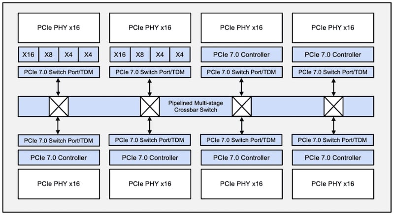
Block diagram of the PCIe 7.0 Switch. Image used courtesy of Rambus
This approach addresses a growing architectural challenge in AI data centers. As systems scale to accommodate larger clusters of GPUs, accelerators, and NVMe storage arrays, the traditional method of provisioning dedicated PCIe connections for each endpoint becomes impractical. Adding more physical lanes means more PHYs on the SoC die, which consumes silicon area, increases power, and complicates routing. TDM offers an alternative by better utilizing existing links, potentially reducing the number of PHYs required in a given SoC design.
The switch supports both disaggregated and pooled compute architectures, two design approaches gaining traction in AI infrastructure. Disaggregated designs separate compute, memory, and storage resources into independent pools that can be composed on demand, while pooled architectures allow multiple hosts to share access to resources like accelerators or storage. Both models depend on a flexible, low-latency switching fabric, and Rambus says the TDM capability maintains deterministic performance even as traffic patterns shift between workload types.
Positioning Within PCIe 7.0
The PCIe 7.0 specification doubles the raw data rate per lane to 128 GT/s, up from PCIe 6.0, reflecting the bandwidth demands of AI training clusters and large-scale storage deployments. As SoC designers begin integrating PCIe 7.0 interfaces, the switch layer becomes increasingly critical for efficiently routing traffic within and between systems.
Rambus has been building out its PCIe 7.0 IP portfolio over the past year, with controllers and retimers already announced. The switch IP extends the lineup into the fabric layer, where data traffic is routed between multiple endpoints. The company says the switch is designed to integrate with leading-edge ASIC platforms and complement its other PCIe 7.0 offerings.
Rambus didn’t announce specific availability dates or name customer engagements for the switch IP. The company, which employs approximately 800 people, has built its business around licensing high-speed interface IP to semiconductor companies designing data center and AI chips. The switch IP launch reinforces its focus on providing the full interconnect stack for next-generation data center silicon.
PCIe Switching for AI
AI infrastructure is increasingly defined by how efficiently data can move between heterogeneous compute and memory resources. Advanced PCIe switching technologies that improve link utilization and enable flexible traffic orchestration will be key to building scalable, cost-effective AI platforms.
The PCIe 7.0 Switch IP with TDM gives architects a way to scale bandwidth efficiently and deterministically while reducing complexity and improving overall system utilization. This may enable it to scale the next wave of advanced AI clusters and HPC networks.