Facebook
 Google
 GitHub
 Linkedin
Transimpedance Amplifier Stability
Learn about how to stabilize transimpedance amplifiers or TIAs with useful examples.
Learn about transimpedance amplifier stability with practical methods and useful examples.
This article covers transimpedance amplifiers and how to stabilize them.
If you'd like to learn more, please check out our article on how to analyze stability in transimpedance amplifiers.
What Is a Transimpedance Amplifier?
We begin by defining what a transimpedance amplifier is. For context, let's take a look at an example circuit.
![]()
(a) (b)
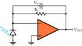
Figure 1. (a) Basic I-V converter, or transimpedance amplifier (TIA). (b) Practical implementation, showing the stray capacitance Cn associated with the op-amp’s inverting input pin.
The circuit of Figure 1(a) accepts an input current Ii and converts it to an output voltage Vo. Aptly called I-V converter, it finds a variety of applications, two prominent ones being as photodiode preamplifier and as a buffer for current-output digital-to-analog converters (DACs). To find the relationship between Vo and Ii, we use Ohm’s law to write Vo – Vn = RIi, and the op-amp law to write Vo = a(0 – Vn) = –aVn, where a is the op-amp’s open-loop gain. Eliminating Vn and solving for the ratio Vo/Ii, we get the closed-loop gain
$$A=\frac{V_{O}}{I_{i}}=\frac{R}{1+\frac{1}{a}}$$
Equation 1
In the ideal op-amp limit a→∞, we have A → Aideal = R. Since A has the dimensions of volts/amperes, or ohms, which are the dimensions of impedance, A is aptly called the transimpedance gain, and the circuit is also known as a transimpedance amplifier (TIA).
A real-life TIA, depicted in Figure1(b) includes also a stray capacitance Cn, consisting of the parasitic capacitances (discussed in a previous article on input capacitance in op-amps) plus the parasitic capacitance of the circuit providing Ii (typically, a photodiode or a current-output DAC). Depending on the application, Cn is typically on the order of 10 pF to 100 pF or higher. Regardless, it is a common tenet that Cn tends to destabilize the TIA, so it is the task of the designer to take suitable measures to stabilize the circuit.
Destabilization in Stray Capacitance: Rate of Closure
Let us investigate the destabilizing tendency of Cn using the rate-of-closure (ROC). To this end, we set the input source to zero, break the loop as in Figure 2(a), apply a test voltage Vt and calculate the feedback factor β(jƒ) as
![]()
(a) (b)
Figure 2. (a) Finding the feedback factor β(jf). (b) Rate of closure (ROC) approaching 40 dB/dec. (Here a0 is the DC gain, ƒb the bandwidth, and ƒt the transition frequency).
$$β(jf)=\frac{V_{n}}{V_{t}}=\frac{\frac{1}{j2πfC_{n}}}{\frac{1}{j2πfC_{n}}+R}=\frac{1}{1+j2πfRC}$$
Equation 2
This is readily put in the form
$$β(jf)=\frac{1}{1+\frac{jf}{f_{p}}}$$
Equation 3
where
$$f_{p}=\frac{1}{2πRC_{n}}$$
Equation 4
Physically, Cn and R establish a pole frequency within the feedback loop. Consequently, a signal traveling around the loop will have to contend with two poles, one due to the op-amp and the other due to Cn, with the risk of a phase shift approaching 180° and thus jeopardizing circuit stability. We can better visualize this in Figure 2(b), which shows the plots of the open-loop gain |a| and the reciprocal of the feedback factor |1/β(jƒ)|, where
$$\frac{1}{β(jf)}=1+\frac{jf}{f_{p}}$$
Equation 5
The pole frequency ƒp of β(jƒ) is a zero frequency of 1/β(jƒ), indicating that the |1/β(jƒ)| curve starts to rise at ƒp. If ƒp is low enough compared with the crossover frequency ƒx, the ROC will approach 40 dB/dec, indicating a phase-margin approaching zero.
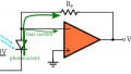
A common cure for combating the phase lag due to Cn is to introduce phase lead by means of a feedback capacitance Cƒ across R, as depicted in Figure 3(a).
![]()
(a) (b)
Figure 3. (a) Combating the phase lag due to Cn by means of the phase-lead introduced by Cƒ. (b) Imposing ƒz = ƒp for a phase margin ɸm ≈ 45°.
Equation (2) still holds, provided we replace R with Z(jƒ) = R||[1/(j2πƒCƒ)]. This gives, after some algebraic manipulation,
$$\frac{1}{β(jf)}=\frac{1+\frac{jf}{f_{p}}}{1+\frac{jf}{f_{z}}}$$
Equation 6
where
$$f_{p}=\frac{1}{2πR(C_{n}+C_{f})}$$ $$f_{z}=\frac{1}{2πRC_{f}}$$
Equation 7
Note that Cƒ creates a zero frequency ƒz for β(jƒ), while also lowering the existing pole frequency ƒp somewhat (recall that a pole/zero for β becomes a zero/pole for 1/β).
An easy-to-visualize technique specifies Cƒ so as to position ƒz right at ƒx, as in Figure 3(b). This reduces the ROC from about 40 dB/dec to about 30 dB/dec, thus ensuring a phase margin of about 45°. To find the required Cƒ, we note from Figure 3(b) that ƒz equals the geometric mean of ƒp and ft, that is, ƒz = (ƒp׃t)1/2. Using the expressions of Equation (7) and simplifying gives
$$C_{f}=\sqrt{\frac{C_{n}+C_{f}}{2πRf_{t}}}$$
Equation 8
This transcendental equation is readily solved by iterations, as shown next.
A Photodiode Preamplifier Example
The circuit of Figure 4 typifies a photodiode preamplifier, such as those used in light detection and ranging (LiDAR).
![]()
Figure 4. Photodiode preamplifier with compensation for a phase margin ɸm ≈ 45°.
Incident light causes the photodiode to draw a small current (up to a few microamperes), which the op-amp then converts to a useable voltage. The op-amp is assumed to have a constant gain-bandwidth product of 10 MHz, and the total stray input capacitance (sum of the diode’s junction capacitance and the stray capacitances of the op-amp, circuit components, and circuit traces) is assumed to be 50 nF. The value of Cƒ is found via Equation (8). Start out assuming Cƒ = 0 and get
$$C_{f}=[\frac{(50+0)×10^{-12}}{(2π10^{6}×10^{7})}]^{1/2}=0.892pF$$
Iterate as Cƒ = [(50 + 0.892)×10–12/(2π106×107)]1/2 = 0.900 pF. Another iteration gives again 0.900 pF, so we stop at this value.
Next, let us verify our findings via PSpice. Using the circuit of Figure 5(a) we obtain the plots of Figure 5(b).
![]()
(a) (b)
Figure 5. (a) PSpice circuit to plot |a| and |1/β| for the TIA of Figure 4. (b) The |1/β| curves for the uncompensated (Cƒ = 0) and the compensated (Cƒ = 0.9 pF) cases.
For the uncompensated case we measure ƒx = 178.4 kHz, and the phase angles ph[a(jƒx)] ≈ –90° and ph[1/β(jƒx)] ≈ 89.0°, so the phase margin is
$$ɸ_{m}=180º+ph[a(jf_{x})]-ph[\frac{1}{β(jf_{x})}]≈180-90-89=1º$$
Equation 9
indicating an almost oscillatory circuit.
For the compensated case we measure ƒx = 224.8 kHz, and the phase angles ph[a(jƒx)] ≈ –90° and ph[1/β(jƒx)] ≈ 37.4°, so the phase margin is now ɸm = 180 – 90 – 37.4 = 52.6°, a bit better than the desired ɸm = 45°. The above findings are confirmed by the closed-loop transient responses of Figure 6. Without compensation, the circuit gives a slow-decaying oscillation, whereas compensation tames the oscillation dramatically (what a 0.9 pF capacitor can do!).
![]()
(a) (b)
Figure 6. (a) PSpice circuit to plot the step response of the TIA of Figure 4. (b) The |1/β| curves for the uncompensated (Cƒ = 0) and compensated (Cƒ = 0.9 pF) cases.
The compensated response still exhibits some ringing, and the AC response (shown in Figure 8 below) exhibits some peaking. To eliminate peaking, ɸm must be raised to 65.5°, and to eliminate ringing it must be raised to 76.3°. (For this, I am referencing my book, Design with Operational Amplifiers and Analog Integrated Circuits, 4th Edition.)
Raising ɸm above 45° will result in the situation depicted in Figure 7.
![]()
Figure 7. – Linearized diagram showing the 1/β curve for ɸm > 45°.
Using the PSpice circuit of Figure 5(a), we find by trial-and-error that the required values of Cƒ are as follows:
For ɸm = 45.0° use Cƒ = 0.738 pF and get ƒx = 209 kHz
For ɸm = 60.5° use Cƒ = 1.098 pF and get ƒx = 248 kHz
For ɸm = 73.3° use Cƒ = 1.606 pF and get ƒx = 326 kHz
The corresponding closed-loop responses are shown in Figure 8.
![]()
Figure 8. – Closed-loop (a) AC responses and (b) transient responses of the circuit of Figure 4.
As usual, the price for an increased phase margin is a reduced AC bandwidth and a slower transient response.
TIA Using a Current-Feedback Amplifier (CFA)
The stray inverting-input capacitance has a destabilizing effect also on TIAs based on current-feedback amplifiers (CFAs), as depicted in Figure 9.
![]()
(a) (b)
Figure 9. (a) CFA-based TIA, and (b) compensation for a phase margin of about 45.0°.
This topic is covered in a previous article on dual CFAs and composite amplifiers, where it is shown that the required feedback capacitance for ɸm ≈ 45.0° is
$$C_{f}=\frac{1}{R_{F}}\sqrt{\frac{r_{n}C_{n}}{2πf_{t}}}$$
Equation 10
TIA Using a T-Network
As discussed in connection with Equation (1), the transconductance gain, in the limit a →∞, is Aideal = R. There are applications requiring much higher values of R than 1 MΩ, values that may prove physically impractical. A popular trick around this conundrum is to interpose a voltage divider R1-R2 between the op-amp output and the feedback resistance R, as depicted in Figure 10(a).
![]()
(a) (b)
Figure 10. (a) TIA with a T-network. (b) The voltage divider reduces the effective transition frequency from ƒt to ƒt/(1 + R2/R1).
The voltage at the node common to the three resistances is still, ideally, RIi. The op-amp then magnifies this voltage according to the gain expression of the noninverting configuration, in this case, 1 + R2/(R||R1), so
$$A_{ideal}=(1+\frac{R_{2}}{R||R_{1}})R=mR$$
Equation 11
We are in effect witnessing a resistance multiplication by a factor of
$$m=1+\frac{R_{2}}{R_{1}}+\frac{R_{2}}{R}$$
Equation 12
With the component values shown, m = 1 + 9/1 + 9×10³/106 ≈ 10, so we are achieving Aideal = 107 V/A with a physical resistance of only 106 Ω. As depicted in Figure 10(b), the voltage divider shifts the baseline from 0 dB to +20 dB. Comparison with Figure 3(b) reveals that we are now dealing with an effective transition frequency of ƒt/10, or 1 MHz. Equation (8) still holds, provided we use 1 MHz for ƒt, so Cƒ must be made 101/2 times as large. For ɸm ≈ 45° we calculate Cƒ = 0.900×101/2 = 2.85 pF.
The more refined value of Cƒ = 2.26 pF shown in Figure 11(a) is found by trial and error, as usual.
![]()
(a) (b)
Figure 11. Simulating a TIA with a T-network. Using trial-and-error to find Cƒ for ɸm = 45°.
Practical considerations
The above examples indicate rather small values of Cƒ, typically in the range of picofarads or even sub-picofarads. Such small values may prove physically impractical, so we start out with a more practical value, such as Cƒ = 10 pF, and then we force the op-amp to drive Cƒ via a voltage divider to scale Cƒ down to the (smaller) desired value. This is depicted in Figure 12 for the case ɸm = 45.0°.
![]()
(a) (b)
Figure 12. (a) Simulating a TIA with the capacitance divider R1-R2. (b) Plots of |a| and |1/β| after R2 has been fine-tuned for ɸm = 45°.
As seen earlier, this requires an effective capacitance of 0.738 pF, so we need to impose
$$0.738=\frac{R_{1}}{R_{1}+R_{2}}10$$
Letting R1 = 1 kΩ, we need R2 = 12.6 kΩ. Starting out with this value, and then fine-tuning it by trial-and-error to achieve ɸm = 45.0°, we end up with the value 11.4 kΩ, as shown in Figure 12. Clearly, the voltage divider provides the additional advantage of capacitance tuning via resistance tuning.
Figure 12b reveals also a high-frequency rise of the |1/β| curve, but this is inconsequential if we manage to keep it sufficiently above ƒx. We achieve this by imposing R1||R2 << R.
I hope this article has helped you gain a better understanding of how to stabilize transimpedance amplifiers.
If you'd like more articles like these, please let us know what you'd like to learn in the comments below.
Related Content