Facebook
 Google
 GitHub
 Linkedin
DC-DC Buck Converter Design Tips and Tricks
This article will go over some general tips you can use when designing a DC-DC buck converter.
This article will go over some general tips you can use when designing a DC-DC buck converter.
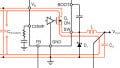
The Basic DC-DC Buck Converter Circuit
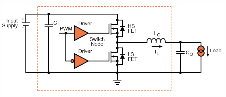
Before we begin, let’s review the circuit of the DC-DC buck converter:
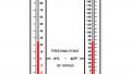
Component Trade-Offs in Buck Converters
It’s important to understand the design trade-offs that you’re faced with.
To help you, I developed a matrix of “what affects what” in buck design:

“What Affects What” by George Biner.
The main trade-off is the choice of inductance (inversely related to k-factor, i.e., the ratio of peak-to-peak to average inductor current), output capacitance, and switching frequency to achieve adequate ripple and transient response.
Designers should definitely take advantage of regulator IC manufacturers’ design tools to determine component values and for circuit simulation as well.
Get to Know Your Capacitors
- Make sure capacitors have capacitance at the frequency of operation and know where their self-resonant frequency is.
- Ceramics are good over wide frequencies but have relatively low capacitance. Usually, one capacitor type cannot cover the entire frequency range and two types (ceramic and electrolytic, for example) must be used in parallel, with the ceramic closer to the circuit.
- Capacitors also lose a lot of rated capacitance with applied bias voltage.
Trust But Verify: Chips and Components
- On PCBs made by third parties with tiny, unmarked components, you must trust the board stuffer that the correct components were installed. Make sure your trust is not misplaced.
- If you’ve sent a chip into the manufacturer for a failure analysis, don’t be inactive waiting for the result. Chip quality levels these days are very high and it’s extremely unlikely that the chip came to you bad. That analysis will also take some time. Meanwhile, you could be finding the real problem.
- If you are using a digital chip, verify that settings you have changed have actually been written into the chip, not just into the GUI.
Consider Test and Measurement
- Don’t assume DC voltages are stable without verifying with a scope.
- There’s a lot to the process of measuring ripple—and the proper equipment to perform it is expensive. While it’s best to use a fancy differential probe, you can use a single-ended probe—just make sure the ground wire is very short and connected right next to Vout.
- Use a 1x probe (you can build it yourself). A 10x probe will not have the sensitivity you need.
HF spikes couple to the output through the parasitic capacitance of the inductor. You may need to slow down the turn-on of the upper MOSFET to reduce ringing or dv/dt spurious turn-on of the bottom MOSFET, although this dings efficiency.
Analyze Your Input Capacitance
- Input capacitance is less understood than output capacitance, but it may be needed to achieve input noise requirements and to make sure your circuit is not starved for current.
- Input capacitors have large ripple currents which peak at 50% duty cycle, create heat, and shorten the cap’s lifetime. Make sure that current is within their spec. There is a basic tradeoff when you add more parallel Cin, as the ever-lower ESR will cause higher ripple currents and more heating. To really get the input ripple current down, you may need a series inductor.
- As duty cycles are higher, the current draw from Cin is higher, resulting in more Vin droop at the chip—this becomes significant if Vin is already low as you are closer to running into the lower Vin limit—you may need to add Cin in these cases.
Think Ahead to PCB Layout
- Know the basics of current paths and minimization of high-current loops. Schools teach a lot about forward circuit paths, but nothing about return paths, which are shown as perfect ground symbols! Make the layout such that return currents can follow their natural paths (which are minimized loops).
- Keep the power path inductances low. Pulsing currents through them create voltage spikes and radiated EMI. High-power vias are OK but their characteristics should be understood.
- Get a sense of the impedance level of circuit nodes and protect them accordingly. For example, the summing node of an error amp is high impedance and sensitive to noise – isolate it and make it small.
- Respect the partitioning between analog, digital, and power grounds and provide natural return paths. Star grounding avoids running big, pulsing currents through ground paths shared with sensitive, low-level circuits.
Know (and Respect) Your Limits
- Make sure you respect the thermal derating curves—at high temp, maximum current and power dissipation are always reduced from the “headline” values.
- Make sure pin voltages are never driven beyond operating specs, both pin to ground and pin to pin. For example, energizing one pin within its pin-to-ground spec, but violating its pin-to-pin spec to a different pin may burn the chip.
- Note the min/max controllable on and off times of the controller chip and make sure you are not operating it too close to its limits.
Conclusion
To learn more, read my article on common failures in converter design and how to troubleshoot them.