Facebook
 Google
 GitHub
 Linkedin
PCB Layout Tips and Tricks: How to Optimize Your Decoupling Connection
This article explores the somewhat complicated issue of how exactly to connect a decoupling capacitor to a power pin.
This article explores the somewhat complicated issue of how exactly to connect a decoupling capacitor to a power pin.
Related Information
- Clean Power for Every IC: Understanding Bypass Capacitors
- Clean Power for Every IC: Choosing and Using Your Bypass Capacitors
Some aspects of PCB layout don’t change much as you transition from low-frequency designs to high-frequency designs. Advantageous component placement, techniques for moving heat away from high-power components, matching trace width to current-carrying requirements, fine-tuning a stencil for proper reflow soldering—these portions of the layout process are more or less the same whether the board’s signals are in the 1–5 MHz range or the 20–50 MHz range.
High-Frequency Decoupling
One thing that does require special consideration, though, is decoupling. The fundamental concepts don’t change as you move from low frequencies to high frequencies, but the implementation might need some improvements, simply because low-frequency designs will often be fully functional when the bypassing is suboptimal or even downright mediocre. In other words, low-frequency circuits are quite forgiving when it comes to decoupling techniques, and consequently we might develop design habits that really are not appropriate for high-frequency systems.
The issue is the following: In the context of digital circuits, decoupling caps store charge and deliver this charge to ICs to compensate for the transient disturbances created by semiconductor switching action. At low operational frequencies, the capacitor has plenty of time to discharge and then recharge before the IC needs another burst of current. As frequency increases, though, the board designer must attempt to reduce the parasitic resistance and inductance that impede the cap’s ability to supply the required charge.
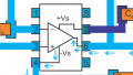
The typical recommendation for decoupling goes something like this: “Use a 0.1 µF ceramic capacitor placed as close to the power pin as possible.” For example:

This advice is a good starting point and is adequate for low-frequency design, though it becomes woefully oversimplified when you start to learn about the complexities involved in high-speed bypassing. In this article, we’ll look at one specific issue that is relevant to high-speed decoupling techniques, and we’ll continue the discussion in another article.
Trace or Via?
We know that we’re supposed to place decoupling caps close to their respective pins, but after you get them nice and close, how do you actually make the connection?
Let’s assume that the power and ground pins are far enough apart that you can’t make a trace connection to both pins. You position the cap such that one terminal is near VDD, and then you connect the other terminal to ground using a via. Should you make the VDD connection using a trace or a via? Well, that’s an easy question to answer if you don’t have a power plane—a trace (or copper pour) is your only option. But honestly, if the board’s frequencies are high enough to make you worried about optimizing your decoupling caps, you really should have a power plane.
For boards that include a power plane, the conclusion of Dr. Howard Johnson, a notable expert in high-speed digital design, is that via connections are far better. The following example is an improvement on the previous diagram, but as you will see in the next article, the via configuration is suboptimal.

You can read his thorough explanation in the High-Speed Digital Design Online Newsletter; my favorite statement was the following: in the context of high-speed digital design, placing any nontrivial length of PCB trace in series with a power terminal “radically increases power supply noise” and “should be avoided like the plague.” I find this interesting because it is somewhat counter-intuitive—the trace just seems more “direct” than connecting the pins through vias.
The Quest for Lower Inductance
This issue is rather nuanced when you delve into the details, but a significant portion of the discussion boils down to inductance, which is such a troublemaker for designers of high-frequency digital systems. By using a via for both the capacitor and the power pin, the conductor that connects the two pins is the power plane, which of course has far less inductance than a typical trace.
You might be wondering, “What about the inductance of the vias?” Does a short trace really have significantly more inductance than two vias?
This app note (page 4) from TI gives the following equation for calculating the inductance of a via:
$$L(nH)=\frac{h}{5}\left(1+\ln\left(\frac{4h}{d}\right)\right)$$
where h is the height in mm and d is the diameter in mm. Let’s say we’re using a 10 mil (= 0.254 mm) drill for the vias and we have the standard 63 mil (= 1.6 mm) PCB thickness. This corresponds to a via inductance of 1.3 nH. Thus, two vias would give us less than 3 nH, compared to about 3.5 nH for a half-inch PCB trace. A 0.5 nH reduction is not too impressive, but this is a very conservative estimate because the current is coming from the power plane, not the bottom side of the PCB. In other words, it doesn’t have to pass through all of the via’s inductance.
Let’s say that the power plane is on the layer adjacent to the IC, and the prepreg thickness is about 10 mils (= 0.254 mm).

Copper-layer separation distances for a typical 63-mil-thick PCB. Based on information published by Advanced Circuits.
Now the calculated inductance is only 0.12 nH, and we can see that the pair of vias can provide performance far superior to that of the trace.
Conclusion
We’ve discussed an important technique for making a high-performance connection between a decoupling capacitor and a high-speed digital IC that is on the same PCB layer. We’ll discuss additional decoupling details in the next article.