Facebook
 Google
 GitHub
 Linkedin
How a Ground Plane Reduces PCB Noise
How does a ground plane reduce noise in a PCB? Learn more in this technical article.
How does a ground plane reduce noise in a PCB? Learn more in this technical article.
Why should you use a ground plane whenever possible in PCB design? A ground plane reduces the inductance of the signal return path. This, in turn, minimizes the noise from transient ground currents.
In this article, we'll discuss how a signal path functions on a multi-layer PCB and the concept of return path inductance.
The Signal Chooses the Path of Least Impedance
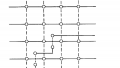
Consider a two-layer board as shown in Figure 1. The bottom layer is a ground plane and a current source is connected to a U-shaped trace on the top layer. The top layer trace is connected to the bottom layer through VIA1 and VIA2.
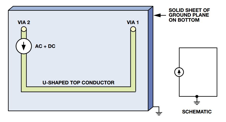
Figure 1. Image courtesy of Analog Devices.
First, as shown in Figure 2, a DC current is injected into the top layer trace.
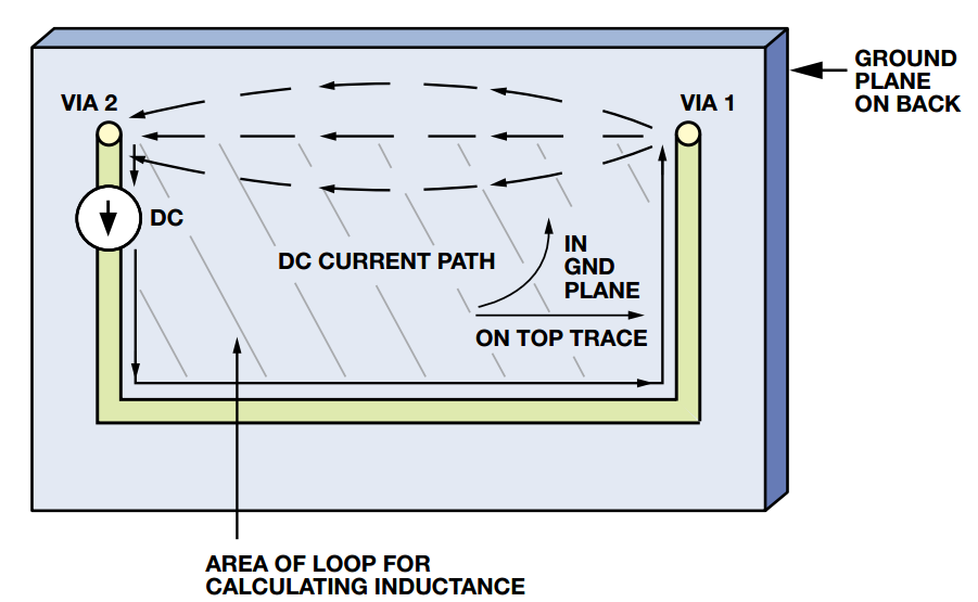
Figure 2. Image courtesy of Analog Devices.
The current goes down the U-shaped trace. Then, through VIA1, it reaches the ground plane. What part of the ground plane will conduct the current back to VIA2? We can envision the ground plane as an infinite number of narrow traces that are in parallel. The current will choose the traces that exhibit a relatively smaller impedance. Since the direct path from VIA1 to VIA2 is the shortest and has the least resistance, most of the current will flow through this path. As we move away from this path of least resistance, the current density will rapidly decrease.
Now, assume that we inject an AC current into the U-shaped trace.
Will it take the same path the DC current did?
The DC current took the path of least impedance (or least resistance). For an AC current, the impedance depends on both the resistance and inductance of the path. While the shortest path offers the least resistance, it doesn’t necessarily offer the least inductance. The inductance of a path depends on the area of the loop created by the current flow. Figure 3 shows an example current loop that the signal trace and its return path created. If the area of the loop made by the current flow increases, the inductance will increase proportionally.

Figure 3. Image courtesy of Analog Devices.
For example, the red return path in Figure 4 creates a larger loop than the green path. Hence, between these two paths, the AC current goes through the green path, which has a smaller inductance. For the overall impedance of a path, we should actually consider both the resistance and inductance. However, as the frequency of the AC signal increases, the contribution of the inductance to the path impedance eventually becomes orders of magnitude greater than that of the resistance. Hence, as shown in Figure 4, the high-frequency return current will flow directly underneath the U-shaped trace to minimize the loop area (we’re ignoring the path resistance for simplicity). As we move away from this path in the ground plane, the current density will rapidly decrease.
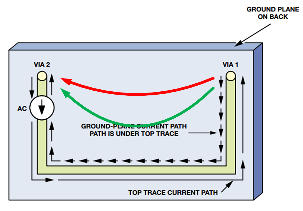
Figure 4. Image courtesy of Analog Devices
For the above example, we have a ground plane that can be envisioned as an infinite number of narrow parallel paths. The return current flows through those paths that minimize the impedance. With a two-layer board, we cannot afford a ground plane. In this case, we may have a single track (rather than a plane) for the return current. The current is forced to go through this path, even though it may exhibit significant inductance. For a few critical signal traces of a two-layer board (such as clock signals), we can route an appropriate return path, but we cannot do this for all of the traces on the board. How can we reduce the current-path inductance for all the traces on a double-sided board? We’ll soon discuss an efficient ground system for two-layer boards, but before that let’s take a brief look at the mechanisms by which the ground path inductance increases the board noise.
Why Is Return Path Inductance Important?
A simple model for the return path inductance can be obtained by putting an inductor in series with the ground of the circuit schematic. An example is shown in Figure 5. Assume that the output of gate 1 goes from logic high to logic low. This will discharge the electric charge stored in CSTRAY through the ground path. Considering today’s fast logic gates, the discharge will take place in a short period of time (∆t). The discharge current will flow through the ground inductance. If the current through the inductor changes by ∆I during the logic transition, the ground of the logic gates will bounce by $$V =L\frac {∆I}{∆t}$$.
In this case, the output of the gates that are at logic low (gate 2 in Figure 4) will experience a noise voltage pulse. If large enough, this noise voltage can lead to an unwanted transition at the output of gate 4.
Moreover, as shown in Figure 4, the ground noise voltage can be coupled to the cables that leave the PCB. Acting as an antenna, these cables can radiate and cause EMC problems.
Figure 5 reveals another interesting mechanism by which the ground inductance can cause problems. When the output of gate 1 transitions from logic high to logic low, the transistors inside gate 1 connect the stray capacitance to the inductor created by the ground path. If the transistor connecting CSTRAY to the ground inductance exhibits a small resistance, a high-Q series resonant circuit will be created. This can lead to logic gate transitions with considerable ringing. If we cannot reduce the ground inductance sufficiently, we may need to add a resistor (e.g., 51 Ω) in series with the gate output to dampen the ringing.
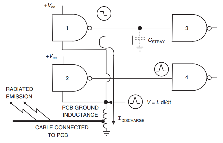
Figure 5. Image courtesy of Electromagnetic Compatibility Engineering.
The above noise mechanisms show that ground path inductance is of paramount importance when designing a PCB. As discussed before, a multi-layer board allows us to have solid ground planes, which can significantly reduce the ground inductance. However, with a double-sided board, we have to resort to other techniques to implement a low-inductance ground system.
To see a complete list of my articles, please visit this page.
Related Content