Facebook
 Google
 GitHub
 Linkedin
How to Reduce Ground Bounce: Mitigating Noise with PCB Design Best Practices
Learn what ground bounce is and how you can avoid it with design decisions from PCB layout to programming.
Learn what ground bounce is and how you can avoid it with design decisions from PCB layout to programming.
PCB design is not taught to most undergraduate engineers. From a certain perspective, previous generations of electronics were rather forgiving and design errors would still allow you to create a functional board. We know this because, if you spend much time in this business looking at schematic diagrams and PCB designs made by others, you will quickly find oversights, mistakes, and glaring errors on production PCBs. You may even find mistakes in your own past designs.
These mistakes have slipped through in part because oftentimes the boards work anyway—even if just barely.
But, as we progress to smaller, faster, lower-power circuits, it will very much matter how we create circuit boards. As Dr. Eric Bogatin—Teledyne LeCroy physicist and self-proclaimed "Signal Integrity Evangelist" puts it:
"Use best design practices unless you have a compelling reason not to.”
This article provides information on the causes of ground bounce and some best practices for how you can mitigate it in your designs.
What Is Ground Bounce?
Ground bounce is a form of noise that occurs during transistor switching when the PCB ground and the die package ground are at different voltages.
To help explain the idea of ground bounce, take the example of the push-pull circuit below that can provide either logic-low or logic-high output.

Figure 1. A push-pull circuit
The circuit consists of two MOSFETs: The upper p-channel MOSFET has its source connected to Vss and the drain connected to the output pin. The lower n-channel MOSFET has its drain connected to the output pin and its source connected to ground.
These two MOSFET types have opposite responses to MOSFET gate voltages. An input logic-low signal at the MOSFET gates will cause the p-channel MOSFET to connect Vss to Output and the n-channel MOSFET to disconnect Output from Gnd. An input logic-high signal at the MOSFET gates will cause the p-channel MOSFET to disconnect its Vss from Output and the n-channel MOSFET to connect Output to Gnd.
Connecting the pads on the IC die to the pins of the IC package are tiny bonding wires. These mechanical necessities have a small amount of inductance, modeled by the simplified circuit above. There is certainly some amount of resistance and capacitance in the circuit, as well, that are not modeled nor necessarily needed to understand the following overview.
Three inductors are shown in the equivalent circuit for a full-bridge switch. The inductor symbols represent the package inductance (inductance inherent in an IC's package design) and the circuit output is connected to some components (it is not allowed to float).
Imagine encountering this circuit after the input is held at logic low after a long period of time. This state would have caused the upper transistor to connect the output of the circuit to Vss through the upper MOSFET. After a suitably long period of time, stable magnetic fields would exist in LO and LA, and the potential difference for ΔVO, ΔVA, and ΔVB is 0 Volts. A small amount of charge will be stored in the trace.
As soon as the input logic switches to low, the upper MOSFET would disconnect Vss from the output, and the lower gate would trigger the lower MOSFET to connect the output of the circuit to GND.
This is where the interesting things happen—at the moment the input logic changes and the consequences move throughout the system.
Causes of Ground Bounce
The potential difference between output and ground causes current to move down from the output to ground through the lower MOSFET. The inductors use the energy stored in their magnetic fields to establish a potential difference up and across ΔVO and ΔVB that try to resist changes in the magnetic field.
Even though they are electrically connected, the potential difference between the output and ground is not immediately at 0 V. Remember that the output was previously at Vss and the source of MOSFET B was previously at 0 V potential. This previous potential difference will cause current to flow while the output line discharges.
At the same time that current is starting to move from the output down to ground, the inductive properties of the package create a potential difference across ΔVB and ΔVO to try to maintain the previously established magnetic field.
The inductors LB and LO change the MOSFET source and drain potentials. That is a problem because the MOSFET gate voltage is referenced to the ground on the die-package. The input voltage might no longer be sufficient to keep the gate open or cause it to open multiple times as the circuit oscillates near the gate trigger threshold.
When the circuit switches again, a similar set of circumstances will cause a potential to be established across ΔVA that decrease the source voltage of MOSFET A below a triggering threshold.
Why Is Ground Bounce Bad?
At the moment that the input changes state, the output and MOSFETS are no longer in a defined state—they are somewhere in between. The result might be false switching or double-switching. Additionally, any other parts on the IC die that share the same Gnd and Vss connections will be impacted by the switching event.
But the effects of ground bounce are not limited to the IC die. Just as ΔVB forces the MOSFET source potential above 0V, it forces the circuit Gnd potential below 0 V. Most of the images you see depicting bounce show the external effects.
If you have several gates switching at the same time, the effect is compounded and can completely disrupt your circuit.
You can see bounce in the examples below.
Significant Gnd and Vss bounce is shown in Figure 2 in a signal line from the BeagleBone Black computer with the LightCrafter cape attached and activated.
Here, approximately ~1V of noise is generated on a 3.3V line during switching that continues to resonate appreciably in the signal lines before eventually falling into the background line noise.

Figure 2. A signal line from the BeagleBone Black with the LightCrafter cap attached and activated.
The noise is not limited to the gates that are switching. The switching gates connect to the ICs power pins, and PCBs often share common power and ground rails. That means that the noise is easily communicated to other places in the circuit either through direct electrical connection via Vss and Ground on the die or coupling of the traces on the PCB.

Figure 3. This image is captured from the BeagleBone Black with the LightCrafter cape attached.
In Figure 3, Channel 2 (shown in cyan above) shows ground and Vss bounce in an undamped signal line. The problem is significant enough that it telegraphs through to a different signal line on Channel 1 (shown in yellow).
Methods for Decreasing Ground Bounce: PCB Design Tips
Method #1: Use Decoupling Capacitors to Localize Ground Bounce
The go-to solution for decreasing ground bounce is to install SMD decoupling capacitors between every power rail and ground as close to ICs as physically possible. Distant decoupling capacitors have long traces that increase inductance, so you do yourself no favors by installing them far from your IC. When the transistors on the IC die switch state, they will change the electrical potential of the transistors on the die and the local power rails.
Decoupling capacitors provide a temporary, low impedance, stable potential for the IC and localize the bounce effect to keep it from spreading to the rest of your circuit. By keeping the capacitors close to the IC, you minimize the area of inductive loop in the PCB traces and decrease the disturbance.
A note for the new designers out there: Decoupling capacitors are not always shown on schematics and sometimes are not mentioned in datasheets. That does not mean that the design does not require them. Decoupling capacitors are considered so fundamental to a successful design that authors will assume you know that you need them, and sometimes remove them from a schematic to reduce clutter. Choose a 100 nf (0.1 uF) X7R or NP0 ceramic unless the datasheet directs you otherwise.
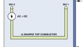
Mixed-signal ICs will often have separate analog and digital power pins. You should install decoupling capacitors on each and every power input pin. The capacitor should be between the IC and multiple vias that connect to the relevant power plane on your PCB.
.jpg)
Decoupling capacitors should be tied to power planes with vias.
Multiple vias are preferred but usually are not possible due to board size requirements. Use copper pours or teardrops to connect vias if you can; the additional copper helps connect the via to the trace if the drill is slightly off center.
.jpg)
Shown above are the copper pads for an IC (U1) and four capacitors (C1, C2, C3, C4). C1 and C2 are decoupling capacitors for high-frequency disturbances. C3 and C4 are added to the circuit per the datasheet recommendation. Via placement is not ideal due to restrictions on other planes.
Sometimes it is physically impossible to place a decoupling capacitor close to an IC. But, if you place it far away from the IC, you create an inductive loop that makes your ground bounce problem worse. Fortunately, there are solutions to this problem.
The decoupling capacitor can be placed on the opposite side of the board underneath your IC.
And, in desperate situations, you can fabricate your own capacitors inside the board using copper on adjacent layers. These are referred to as embedded planar capacitors and consist of parallel copper pours separated by a very small dielectric layer in your PCB. One of the added benefits of this type of capacitor is that the only cost is a designer's time.
Method #2: Use Resistors to Limit Current Flow
Use serially-connected current-limiting resistors to prevent excessive current from flowing into and out of your IC.
Not only will this help your power consumption and prevent you from overheating your device, but it will limit the current that flows from your output lines through your MOSFETs to your Vss and Gnd rails, reducing ground bounce.
Method #3: Use Routing to Reduce Inductance
Keep return paths on neighboring traces or neighboring layers, if possible. The distance between layers 1 and 3 on your board is often several multiples of the distance between layers 1 and 2 due to the presence of thick core material. Any unnecessary separation between the signal and return path will increase the inductance of that signal line and the subsequent effects of ground bounce.
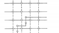
Let's assess a real-world example of a board. In the images below, you can see the PCB layout of an Arduino Uno.
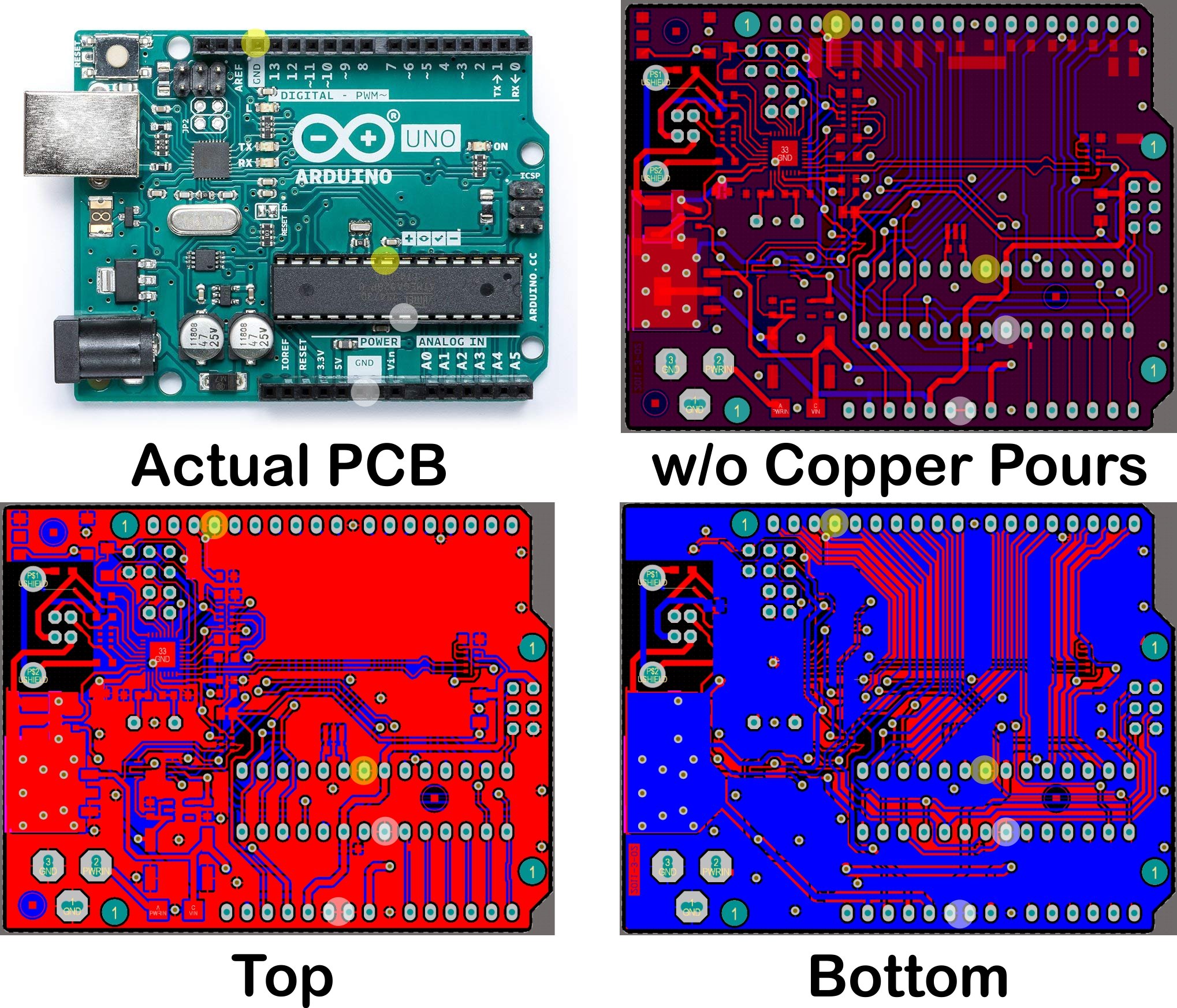
Analog and digital Gnds are highlighted in white and yellow, respectively.
As you can see, the board has separate ground return pins for analog and digital, which is good. However, the layout of the board negates any positive effects of separating them. There is no clear and direct path between the digital ground pins of the IC and the ground pins on the header rows.
Signals will take circuitous routes out of the IC to reach the header pins and a convoluted path to return through the ground pins. Because the Arduino Uno is one of the most popular boards on the planet, this is an excellent example of “it doesn’t matter how you lay out the circuit board.”
If this example piques your curiosity, check out our article on Arduino Uno hardware design.
Reducing Ground Bounce with Programming and Design Considerations
Ground bounce disruption increases as the number of switching gates increases. If possible in your design, offset the switching gates with a short delay.
For example, perhaps you have a design that flashes a variety of LEDs at different intervals (1 second, 2 second, 3 second, etc…) to indicate the status of your design. The ground bounce effect will affect your circuit the most when all three LEDs switch at the same time.
In this example, you could mitigate the effect of ground bounce by slightly offsetting the LEDs so they are not exactly synchronized. Introducing a 1ms offset between the LEDs would be imperceptible to your users, but would reduce the ground bounce effect by a factor of ~3.
Summary for Best Practices
Ground and Vss bouncing are caused by inductive response to fast rise/fall times. You can minimize the effect of ground bounce on your circuit through proper layout and board design practices.
Some methods for reducing ground bounce include:
- Keep decoupling capacitors as close to your IC as physically possible.
- Choose ICs with slower rise/fall times.
- Prevent simultaneous switching when possible.
This article is one of several that were inspired by Dr. Bogatin's keynote address at Altium Live 2018. You can find another such article below:
Related Content