Facebook
 Google
 GitHub
 Linkedin
Guide to PCB Design: How to Generate Manufacturing Files for Custom Printed Circuit Boards
In this article, we'll go over the basics of generating manufacturing files for PCB design and manufacturing.
In this article, we'll go over the basics of generating manufacturing files for PCB design and manufacturing.
When you’re working on a PCB layout, you are editing a file that is specific to your CAD software. It’s not a universal file format, and it uses information that the PCB manufacturer does not need. This is why you have to generate a different sort of file (with an exception we'll discuss at the end of the article) when you’re ready to convert the virtual layout into a physical circuit board.
Guide to Ordering and Assembling Printed Circuit Boards
This article is part of a series:
- PCB Schematic and Board Layout
- How to Generate Manufacturing Files for Custom Printed Circuit Boards
- How to Choose a PCB Manufacturer
What Is a Gerber File?
The most widely used file format for PCB manufacturing is called Gerber. When manufacturers request “Gerbers” or “Gerber files,” they are referring to ASCII files that contain Gerber-formatted data. A Gerber file knows nothing about design rules, net connectivity, or component libraries; it is simply two-dimensional artwork that indicates where the manufacturing equipment will place copper, solder mask, or silkscreen. One Gerber file provides information for one PCB feature on one layer. Thus, if you have a two-layer board and each side has copper, solder mask, and silkscreen, you will need six Gerber files. You may also need a separate Gerber file to identify the board outline. The following image shows a screen capture from my CAD tool and corresponding Gerber files.
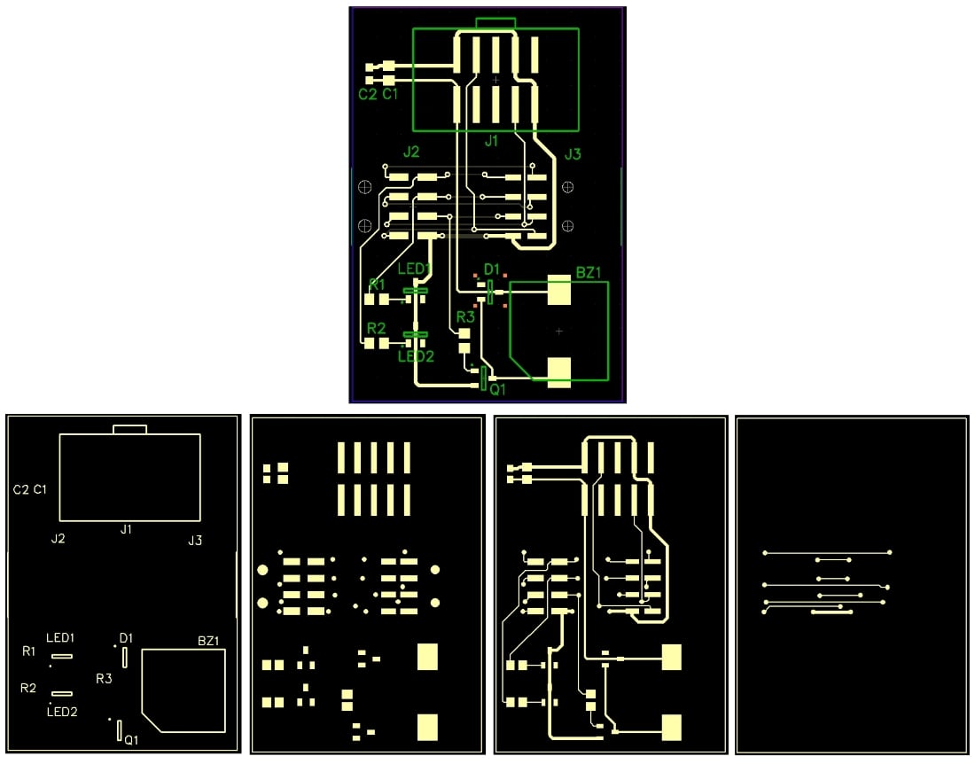
The layout is on the top, and the images in the bottom half represent the Gerber data for (left to right) the top silkscreen, the top solder mask, the top copper, and the bottom copper. I included the board outline in each file (just for visual purposes). This board is a C2 adapter that I designed for programming and debugging Silicon Labs microcontrollers. Click to enlarge.
Generating Gerber files can be somewhat complicated. The process involves various configuration details, and different manufacturers have different requirements. The following screen capture shows the options that you have to consider when generating Gerber files with DipTrace.

If you don’t have much experience with Gerber generation, I suggest the following approach: First, choose a manufacturer that provides specific instructions on how to generate Gerber files with specific CAD tools. Second, use one of these CAD tools to design your board. If you follow the instructions carefully, you will almost certainly avoid the two potential consequences of improper Gerber files: a delay in the manufacturing process (more likely), or a nonfunctional PCB (nowadays probably quite rare).
The Drill File
You will also need to generate a file that indicates the position and size of every hole that will be drilled through your board, i.e., both through-holes (for mounting components) and vias. This is called the NC (numeric control) drill file; you may also see “Excellon drill file” (which comes from Excellon Automation, a company that makes equipment used in PCB manufacturing). Again, the safest approach here is to follow specific instructions provided by a PCB manufacturer.

This image represents the data contained in an NC drill file.
ODB++ vs. Gerbers
Gerber files are universally accepted, and I recommend that you take the time to familiarize yourself with Gerber generation and gradually establish a Gerber routine that allows you to quickly and painlessly create your PCB manufacturing files. However, in some situations it may be better to use ODB++ files. I have to admit that managing multiple Gerber files can be a bit irksome, and this is one advantage of the ODB++ format: it is a single data structure that (in my experience) is generated without extensive input from the designer.
I successfully fabricated one board using ODB++ files, but I also noticed some strange problems that led me back to Gerbers. I’m not saying that the format itself is problematic, but in the end it doesn’t really matter—if my CAD software can’t correctly generate the files or the fab house can’t correctly interpret them, the format is useless to me. If you have had consistent success with ODB++, let us know in the comments section. Honestly, it would probably be beneficial if we all could gradually move away from Gerbers and toward a more straightforward and robust method of packaging and transferring PCB manufacturing data.
Project Files vs. Manufacturing Files
If you’d prefer to avoid generating any type of manufacturing file, you can look for a PCB manufacturer that accepts your CAD software’s project files. I assume that the manufacturer uses some sort of automated procedure to generate Gerbers from the project file; this is beneficial not only because it saves you time but also because the fab house technicians will (presumably) know exactly how to generate files that are compatible with their equipment. The list in the next section gives some information about one manufacturer that accepts project files.
In the next article, we'll talk about choosing a PCB manufacturer to fabricate your design, including assembly options.
Related Content