Facebook
 Google
 GitHub
 Linkedin
6 Ways to Design for Circuit Board Rework
Learn why you should design for rework—and 6 easy ways to do it.
Learn why you should design for rework—and 6 easy ways to do it.
You won’t find DfRwk among any list of DfX design guidelines. DfX refers to a variety of design guidelines collected under the heading “design for excellence.” You’ve probably heard of the more popular guidelines, such as design for manufacturability (DfM), design for assembly (DfA), or design for test (DfT). But how about design for rework (DfRwk)?
DfRwk isn’t yet a part of that family of guidelines, but it should be.

What Does It Mean to Rework a PCB?
For the purposes of this article, rework refers to any operations that need to be completed after the primary printed circuit board assembly operations are complete.
Rework tasks will generally fall into one of two categories:
- Necessary to fix a problem in the design, e.g.:
- You have a schematic symbol that does not coincide with the PCB footprint (which could result in signals being sent to the wrong pins)
- You chose the wrong resistor values.
- You chose the wrong IC
- You forgot to make a necessary connection between two pins (and need to add a jumper wire)
- Necessary to change the design for a specific reason, e.g.:
- You need to create new functionality
- You need to change specs
- You need to switch out components
In the former case, an error was made during design or during assembly, so components or PCB traces need to be changed to fix it. In the latter case, the intended design works, but it turns out to no longer be what is required for the product, so components or PCB traces need to be changed to adjust the design. Primarily, PCBA rework involves heat and solder, though it can also require mechanical operations such as cutting of traces or modifying physical components.
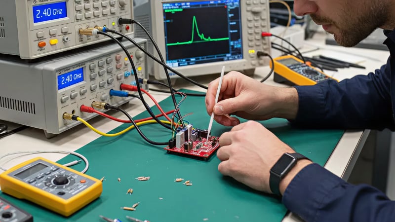
When designing printed circuit boards, you probably don’t think often (if at all) about how your design choices impact future rework operations. But during prototype board bring-up, test, or deployment, rework is often a necessity.
PCB Rework vs. PCB Repair
You may be looking at the above situations and think to yourself that "fixing a problem" in a PCB is the same as PCB repair. The differentiation comes from where errors have occurred. Repair typically occurs when the board has failed for some specific reason. Perhaps there was an ESD strike or a reverse polarity connection. The implication is that the repair is necessary because there has been accidental failure—maybe someone dropped the PCB.
Rework, on the other hand, implies there was a design mistake that needs to be rectified.
6 Tips for Reworking a PCB
Now that we've defined what it means to rework a PCB, let's dive into how it's done! Here are six steps you can take today to improve the DfRwk of your design.
Make Your PCB Larger
Prototypes rarely need to be as small as final designs, so make your prototype PCB larger and put it in an off-the-shelf prototype enclosure. This will allow you to release your design faster, wasting less time on tricky PCB layout issues. To test as part of your system, connect your larger prototype PCB into tight spots in your system using cables. A larger PCB is easier to work with on the bench top, easier to probe, and easier to rework.
Use Larger Components
While it may seem cool and cutting edge to use micro BGA components or 01005 package resistors, you probably don’t need them - and you certainly don’t need them on your prototypes. You cannot easily rework parts that are smaller than a grain of sugar. For prototypes, consider using parts no smaller than 0402 unless absolutely necessary, and using parts with exposed leads instead of BGA or QFN packages, where possible.

In the µModule Product Guide, Linear Tech presents a bitter reminder of just how ugly rework can be. (This is what happens when you don't design for rework.)
Allow More Clearance
Rework is easier and more reliable when there is more clearance around parts. For BGA, QFN, or other packages without exposed leads, allowing ample space around them is critical for localized rework reflow heating. For high-density connectors or press-fit connectors, clearance is necessary for tools that leverage against the PCB. For mechanical components such as heat sink snap-in pins, clearance for hand tools such as pliers is important.
Layout Strapping Resistor and Jumper Options
The goal of circuit designers is to design everything right the first time. But you can save yourself a lot of time and trouble by designing in strapping resistors to allow you to pull all your setting pins high or low with a simple rework. Or consider adding extra unpopulated filter circuits around your power regulators. You can even design in entire secondary circuits that can be implemented by just moving a jumper from one header to another.
Use Programmable Parts
Where possible, use programmable parts to allow rework flexibility. Adjusting firmware is usually easier than cutting traces or re-soldering components. Look for locations where programmable voltage regulators, microcontrollers, or CPLDs/FPGAs might make sense in your prototype, even if it’s not what you intend for your final design. Simple, inexpensive programmable parts allow you to rework your design without risking your hardware.
Install All Programming Headers
Not following this guideline has bitten many, many designers. Spend the extra few cents to install every last one of those pesky programming headers. I can hear you all saying, “But I can program that part through the JTAG chain,” or, “We’ve built that part with the same code for a long time - there’s no chance we’re changing it.” Experience says that you’ll thank me later if you install all of your programming headers on your prototypes.
Follow these six suggestions and your design will be DfRwk ready, saving you time in your schedule and money in your budget.
Related Content