Facebook
 Google
 GitHub
 Linkedin
RTD Signal Conditioning—Voltage vs Current Excitation in 3-wire Configurations
Learn about resistance temperature detector (RTD) signal conditioning techniques such as voltage vs. current excitation and the three-wire configuration for dealing with the lead and wire resistance error.
Previously, we explored the basics of RTDs and touched on RTD signal conditioning circuits. This article dives further into RTD signal conditioning techniques and introduces concepts such as voltage vs. current excitation, as well as the three-wire configuration for dealing with the lead resistance error.
Voltage vs Current Excitation in RTD Applications
Though we used a voltage excitation in the previous article on signal conditioning, it should be noted that most RTD applications use a current source to excite the sensor. Figure 1(a) and (b) depict simplified diagrams for voltage and current excitation methods, respectively.
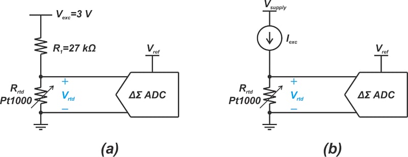
Figure 1. Diagram of voltage (a) and current (b) excitation methods.
The choice between these two methods is at the designer's discretion; however, current excitation can offer better noise immunity and is generally the method of choice in noisy industrial environments. Most delta-sigma (ΔΣ) converters designed for RTD applications include one or more internal current sources for RTD excitation. As a result, current excitation seems to be more common than voltage excitation. We’ll also discuss shortly that it is easier to compensate for the RTD lead resistance error when using current excitation.
RTD Resistance: Wiring Resistance Error
The lead and wiring resistance appears in series with the RTD resistance and introduces errors into our measurements. Assume that a 100 Ω RTD is connected to the measuring system through a 10-feet wire that exhibits a resistance of 1 Ω (at 0 °C) in series with each lead of the sensor, as shown in Figure 2.
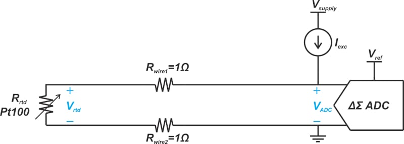
Figure 2. An example diagram depicting lead and wiring resistance.
In this case, the total resistance “seen” by the ADC (analog-to-digital converter) is 102 Ω at 0 °C. Considering a temperature coefficient of 0.385 Ω/°C for the RTD, the wiring resistance introduces an error of 5.2 °C. In practice, the sensor can be further away from the measuring system, leading to a larger error. Moreover, since the wiring resistance changes with temperature, the error is not constant and cannot be easily trimmed out.
The simple wiring configuration shown in Figure 2 is known as the two-wire configuration. Two other wiring techniques, three-wire, and four-wire configurations, allow us to compensate for the wiring resistance error. The two-wire configuration is the simplest and least accurate of the three available options. Note that the lead wire resistance also produces an error in the circuit depicted in Figure 1(a) that uses voltage excitation.
RTD Three-wire Configuration
The three-wire configuration is shown in Figure 3.
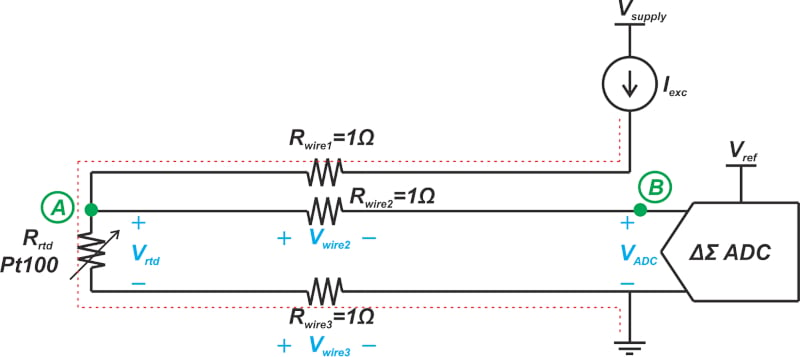
Figure 3. A diagram showing the three-wire configuration.
This configuration requires three wires to connect the sensor to the measuring equipment. The red line shows the current path from the measuring system to the RTD back to the system ground. Assuming that the ADC inputs exhibit high impedance, no current can flow through the wire between nodes A and B. As such, these two nodes are at the same potential, i.e. Vwire2 = 0. Applying Kirchhoff’s voltage law, the voltage that appears at the ADC input is found as:
\[V_{ADC}=-V_{wire2}+V_{rtd}+V_{wire3}=V_{rtd}+V_{wire3}\]
In this case, the resistance from only one of the wires produces an error voltage at the ADC inputs. Assuming that the wires have identical resistances, the above configuration reduces the wire resistance error by a factor of two. Figure 4 shows how a three-wire configuration can be used with a voltage-excited RTD.
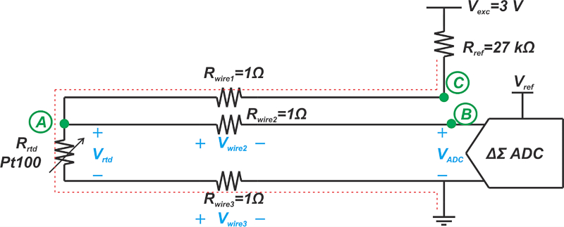
Figure 4. Three-wire configuration example with a voltage-excited RTD.
Again, no current flows through Rwire2, and the ADC senses the voltage across the RTD plus that across Rwire3. This halves the wiring resistance error.
Three-wire Configuration Using Two Current Sources
An alternative three-wire configuration with constant current excitation is shown in Figure 5.
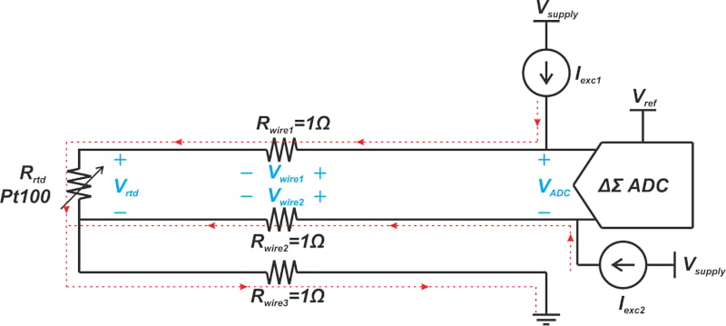
Figure 5. An alternative three-wire configuration with constant current excitation.
In this case, two matched current sources are used to totally eliminate the wire resistance error. Applying Kirchhoff’s voltage law, we have:
\[V_{ADC}=V_{Wire1}+V_{rtd}-V_{Wire2}\]
Assuming that the current sources and the wire resistances are identical (\(I_{exc1}=I_{exc2}\, and \,R_{wire1}=R_{wire2}\)), the same voltage drop appears across Rwire1 and Rwire2, and we have VADC = Vrtd. Therefore, the voltage measured by the ADC eliminates the wire resistance error. The sum of the two excitation currents flows harmlessly through the third wire to the system ground. Some ADCs, such as the AD7711 from Analog Devices, that target RTD applications provide matched current sources to facilitate the above three-wire configuration.
Figure 6 shows the functional block diagram of the AD7711 that contains two matched 200 μA current sources.
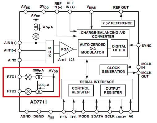
Figure 6. Block diagram for AD7711. Image used courtesy of Analog Devices
The circuit in Figure 5 assumes that the two current sources are identical. Any mismatch between the two current sources allows the wiring resistance to introduce errors into the system. One way to get around this problem is to swap the two currents between the inputs. The voltages obtained from these two configurations are then averaged to remove the current mismatch error. Let’s derive the equations to fully understand how this technique works. First, consider the case shown in Figure 5 and assume that the current sources are unequal. The voltage measured by the ADC can be found as:
\[V_{ADC1}=R_{wire1}I_{exc1}+R_{rtd}I_{exc1}-R_{wire2}I_{exc2}\]
If we swap the two current sources between the two inputs (Figure 7), we obtain a new measurement:
\[V_{ADC2}=R_{wire1}I_{exc2}+R_{rtd}I_{exc2}-R_{wire2}I_{exc1}\]
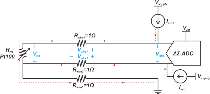
Figure 7. Diagram showing the swap of two current sources between two inputs.
Averaging the two measurements, we obtain:
\[V_{ADC,ave}=\frac{I_{exc1}+I_{exc2}}{2}\Big(R_{wire1}-R_{wire2}+R_{rtd}\Big)\]
If the wire resistances are identical \(R_{wire1}=R_{wire2}\), the above equation simplifies to:
\[V_{ADC,ave}=\frac{I_{exc1}+I_{exc2}}{2}\times R_{rtd}\]
This equation is independent of the wiring resistance. Some ADCs, such as the ADS1220 that are designed with an eye on the RTD measurement requirements, include a multiplexer to swap the internal current sources. Figure 8 shows a three-wire RTD measurement diagram with current swapping (or chopping) capability that uses the ADS1220.
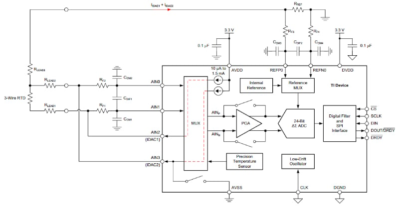
Figure 8. A three-wire RTD measurement diagram with current swapping. Image used courtesy of TI
Improving Accuracy in Three-wire Voltage Excited RTD
With a three-wire configuration, it is possible to use two matched current sources to eliminate the wire resistance error. What about a voltage-excited three-wire RTD? Is there an easy way to totally eliminate the wire resistance error in this case? We discussed above that the voltage-excited three-wire circuit only halves the wire resistance error. We can use the modified diagram depicted below (Figure 9) to eliminate the wire resistance error.
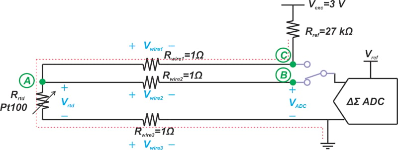
Figure 9. Example diagram showing the elimination of the wire resistance error.
In this case, an analog switch is incorporated that allows us to measure the voltage of nodes B and C. The voltage at node B is given by the following equation:
\[V_{B}=V_{A}=V_{rtd}+V_{wire3}\]
Equation 1.
The voltage at node C is obtained as:
\[V_{C}=-V_{wire1}+V_{rtd}+V_{wire3}\]
Equation 2.
Assuming that the wire resistances are identical, we can conclude that Vwire3 = -Vwire1. Therefore, Equation 2 simplifies to:
\[V_{C}=V_{rtd}+2V_{wire3}\]
Equation 3.
Combining Equations 1 and 3, we obtain:
\[V_{rtd}=2V_{B}-V_{C}\]
As you can see, the voltage drop across the RTD can be accurately measured by measuring VB and VC. Although this technique allows us to compensate for the wire resistance error, it requires additional hardware and increases the complexity of the measurement. ADCs containing matched current sources provide a convenient solution to eliminate the wire resistance error. This is one reason why current excitation is more common than voltage excitation in RTD applications.
To see a complete list of my articles, please visit this page.
Related Content