Facebook
 Google
 GitHub
 Linkedin
Assessing the ADC SNR and SFDR for Communications Systems
In this article, we will see how we can determine the SFDR for an ADC used in a radio receiver. Also, we’ll examine the ADC SNR requirement for this application.
In a previous article, we looked at the different definitions of the spurious free dynamic range (SFDR) specification. The SFDR specification is particularly helpful when dealing with communications systems. For example, the single-tone definition of the SFDR is usually used for characterizing the linearity of an A/D converter utilized in a communications system.
In this article, we will see how we can determine the SFDR for an ADC used in a radio receiver. Also, we’ll examine the ADC SNR requirement for this application. Let’s first review the single-tone SFDR.
Single-Tone SFDR
The single-tone SFDR is illustrated in Figure 1. This figure shows the output of a hypothetical circuit with a single-tone input at \(\omega_{in}\). In addition to the desired output at \(\omega_{in}\), there are several different frequency components (spurs) in the output spectrum. The single-tone SFDR is defined as the ratio of the desired signal amplitude to the largest spur over the bandwidth of interest. This ratio is usually expressed in dB.
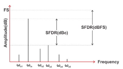
Figure 1
SFDR Can Be Important in Receiver Design
Figure 2 shows an example where the single-tone definition of the SFDR can be used to characterise the system linearity performance. For the purpose of this article, we do not need to go through the details of the analog blocks used in this structure. You can find additional information about these blocks in this article.
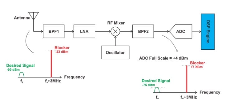
Figure 2
The above figure shows a scenario where the antenna picks up a small desired signal along with a strong in-band blocker. An out-of-band interferer originates from users that belong to a wireless standard other than the one we intend to receive. Such interferers are usually sufficiently suppressed by a band-select filter in the receiver front end. However, the frequency of an in-band interferer is closer to the desired signal and, generally, is removed at the end of the receiver chain. Therefore, in Figure 2, both the desired signal and the in-band blocker will be downconverted to an intermediate frequency (IF), \(f_{IF}\), by the RF mixer. At the output of the RF mixer, we are dealing with much lower frequencies and we can more easily build a relatively high-Q filter, BPF2. Hence, depending on the chosen IF frequency, we may be able to partially suppress the in-band interferer.
However, in Figure 2, we are considering the worst case scenario and we assume that both the desired signal and the in-band interferer experience the same gain (24 dB) from the antenna to the ADC input. The ADC should be able to digitize this input without adding significant distortion. The digital filters within the “DSP Engine” will hopefully get rid of the blocker and keep only the desired signal.
The large blocker can make the ADC nonlinear and lead to spurs at frequencies that are very close to our desired signal. This is depicted by the purple components in Figure 3.
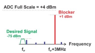
Figure 3
If a spur close to the desired signal is sufficiently large, it can degrade the system signal-to-noise ratio (SNR) to an unacceptable level. Hence, we need to know the largest spur that the ADC can create. This is what the single-tone SFDR quantifies. It allows us to assess how well the ADC can simultaneously process a very small signal in the presence of a large signal.
The ADC SFDR Requirement
Let’s see how we can determine the required SFDR for the example shown in Figure 2. We assume that our wireless standard requires detecting a signal as small as -99 dBm, and the largest in-band blocker that the antenna can pick up is -23 dBm. Both of these two signals will experience the same gain going through the analog blocks in Figure 2. How large can the total gain from antenna to the ADC input be? Assume that the ADC full scale voltage is 2 V and its input impedance is 1000 Ω. We typically lower this impedance using a shunt resistance and match it to the output impedance of the RF/IF system. This is shown in Figure 4.
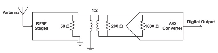
Figure 4. Image adapted from RF and Baseband Techniques for Software Defined Radio.
In Figure 4, the output impedance of the RF/IF system is 50 Ω and a 200-Ω resistor is placed in parallel with the A/D converter. Hence, the transformer should have a turns ratio of 1:2 so as to achieve impedance matching between the “RF/IF Stages” and the “A/D Converter”. Hence, the equivalent resistance at the ADC input is about 200 Ω. For a sine wave with peak-to-peak value equal to the ADC full scale voltage (2 \(V_{p-p}\)), we obtain:
\[P_{ADC}= \left ( \frac {V_{p-p}}{2} \right ) ^2\times \frac {1}{2R}= \frac {1}{400}W\]
This is the maximum power that we can have at the ADC input. In terms of dBm, we have
\[P_{ADC, dBm}=10log \frac {P_{ADC}}{1 mW}=10 log \frac {1000}{400} \approx +4 dBm\]
Since the analog blocks in the signal chain can have some gain variation, we consider a gain margin of 3 dB and assume that the maximum signal power at the ADC input is 4 dBm - 3 dB = +1 dBm.
The largest signal that the antenna can pick up is -23 dBm. This signal gets amplified and produces the largest allowed power (+1 dBm) at the ADC input. Therefore, the gain from the antenna to the ADC input should be 24 dB. Since our wireless standard requires detecting a signal as small as -99 dBm, the smallest signal at the ADC input will be -75 dBm. Having the maximum and minimum signal levels at the ADC input , we can calculate the SFDR of the ADC. We only need to make an assumption about the level of the allowed distortion component. Let’s assume that the distortion component should be 18 dB below the smallest signal that can appear at the ADC input. This is depicted in Figure 5.
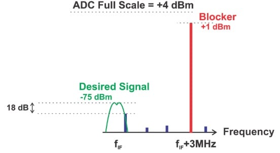
Figure 5
Figure 5 shows that the spur power should be less than -93 dBm. Hence, the ADC SFDR should be larger than 94 dBc. Note that the above analysis assumes that the analog blocks before the ADC are ideal and do not generate any distortion component. Therefore, at the ADC input, we have an amplified version of the signal picked up by the antenna (with no distortion components).
The ADC SNR Requirement
To calculate the required ADC SNR, we need to make some assumptions about the receiver requirements. Assume that our wireless standard mandates having an SNR of about 9 dB at the ADC input to detect the desired signal with an acceptable quality. In other words, if the SNR goes below 9 dB, we’ll have an unacceptable bit error rate. Hence, as shown in Figure 6, the total noise power at the ADC input should be less than -84 dBm.
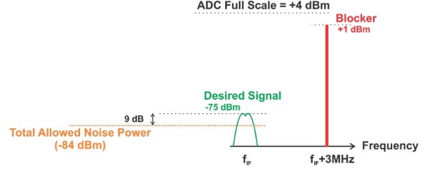
Figure 6
A convenient method to determine the ADC SNR is to choose it sufficiently low so that the analog front end becomes the dominant noise contributor. For example, we can assume that the total noise power generated by the ADC is 12 dB below the noise power allowed by our wireless standard (-84 dBm). Hence, the ADC noise should be less than -96 dBm (as shown in Figure 7). Since the full scale power of the ADC is +4 dBm, its SNR should be greater than 100 dB. We’ll see below that it is possible to use an ADC with much lower SNR.
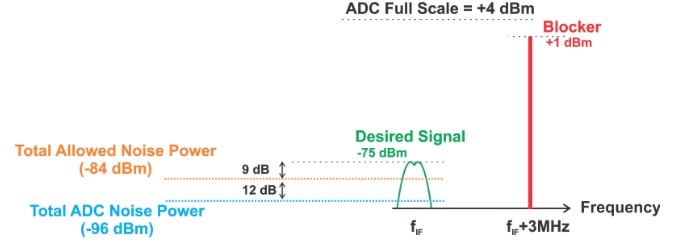
Figure 7
Theoretically, the minimum sample rate of an ADC (\(f_{sample} \)) can be as low as twice the bandwidth of its input signal (BW). However, if we choose the ADC sample rate much larger than twice the bandwidth of its input, we can apply digital filtering (after A/D conversion) to improve the SNR. In this case, the digital filter suppresses the noise outside the desired frequency band. The increase in SNR caused by the oversampling mechanism (along with digital filtering) is often referred to as “process gain”. It can be shown that the process gain is given by:
\[Process \:Gain = 10 log \left ( \frac {f_{sample}}{2BW} \right )\]
For example, if BW=30 kHz and we choose \(f_{sample}\)=65 MSPS, the SNR will improve by 30.34 dB. Assume that the ADC in Figure 2 uses a sample rate much larger than twice the bandwidth of the desired channel so that we have a process gain of about 30 dB. This will relax the ADC SNR requirement from 100 dB to 70 dB.
Note that the above analysis assumes that the ADC noise is much less than the noise that is generated by the analog blocks. If the ADC noise is not negligible, we’ll have to deal with a bit more complex mathematics. Refer to Section 3.3.5.3 of this book for an example that calculates the required ADC SNR without assuming that analog front end is the dominant noise contributor.
Conclusion
In this article, we examined the SNR and SFDR requirements for an ADC used in a communications system. The SFDR specification determines how well the ADC can simultaneously process a very small signal in the presence of a large signal. For the example discussed here, the ADC SFDR should be larger than 94 dB. Making some assumptions about our wireless standard requirements, we obtained an ADC SNR of 70 dB. It’s important to note that based on system requirements, one of these two specifications (either the ADC SNR or SFDR) can be the limiting factor.
To see a complete list of my articles, please visit this page.