 Facebook
 Google
 GitHub
 Linkedin
ADC Resolution vs. Accuracy—Sub-range ADCs, Two-step ADCs, and TUE
Learn about characterizing different analog-to-digital converter (ADC) error sources such as resolution and accuracy.
To ensure that a system meets the required accuracy specification, it is important to have a thorough understanding of different error sources. One of the most critical elements that determine the signal chain accuracy is the A/D converter (ADC), which is the focus of this article. Keep in mind that the accuracy of an ADC can be characterized in terms of absolute accuracy, relative accuracy, and total unadjusted error (TUE).
A common question that is occasionally a source of confusion for young engineers is: how is accuracy related to resolution? For example, is my 12-bit ADC also 12-bit accurate? In a previous article on the differential nonlinearity (DNL) error specification, we briefly discussed that resolution and accuracy characterize two different aspects of an ADC.
ADC Design Parameter—Resolution
The resolution specifies the number of steps in the ADC’s characteristic curve. For an ideal ADC with uniform steps, the resolution determines the minimum change in the analog input voltage that makes the output change by one count. For example, an ADC with 12-bit resolution could resolve 1 part in 212 (1 part in 4096). In other words, a 12-bit ADC can detect voltages as small as 0.0244% of the full-scale value. However, this doesn’t mean that the conversion error (the difference between the input and analog equivalent of the ADC output) is less than 0.0244%.
Resolution is mainly a design parameter rather than a performance specification. It doesn’t specify the conversion error that is actually determined by non-ideal effects such as the ADC nonlinearity, offset, and gain errors.
ADC Accuracy: When Accuracy is Lower Than Resolution
In the context of data converters, it is common to express the accuracy in terms of the number of bits. For example, we might say this ADC is 12-bit accurate. This means that the conversion error is less than the full-scale value divided by 212. In other words, the conversion error is less than one LSB (least significant bit).
With that in mind, this might not be an accurate way of expressing the accuracy of performance because it is not clear what error sources are actually included in this characterization. However, it seems to be normally referring to the combined effect of offset, gain, and integral nonlinearity (INL) errors. The accuracy of a converter can be much lower than its resolution.
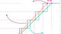
As an example, consider the 12-bit ADC shown below in Figure 1.
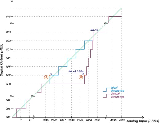
Figure 1. Example of a 12-bit ADC.
In this figure, the blue and purple curves are, respectively, the ideal and actual characteristic curves. In this particular example, the offset and gain errors are calibrated out. The width of code 7FD is 5 LSBs, which leads to an INL error of 4 LSBs at code 7FE. The error in this code is given by:
\[Error=4 \text{ }LSBs=4 \times \frac{Full \text{ }Scale}{2^{12}}\]
Equation 1.
This can be simplified to:
\[Error=1 \times \frac{Full \text{ }Scale}{2^{10}}\]
Equation 2.
Since the conversion error equals the full-scale value divided by 210, we say its accuracy is 10 bits. The above graphic should help you better understand this. First, note that for a given full-scale value, the steps of a 10-bit system are 4 times wider than the steps of a 12-bit system. While the difference between points A and B is 4 LSBs in a 12-bit system, it is only 1 LSB in a 10-bit system. Therefore, Equations 1 and 2 tell us that the error introduced by a 12-bit system that has an INL of 4 LSBs is equal to the error produced by a 10-bit system that has only 1 LSB of INL.
From the INL error point of view, these two systems have identical performance. However, this doesn’t mean that these two systems are exactly the same. For example, the maximum quantization error of the 12-bit system is four times smaller than that of the 10-bit system (or the quantization noise power of the 12-bit system is 16 times smaller).
To more easily calculate the accuracy, we can use the following equation:
\[Accuracy = Resolution -log_{2}(Error)\]
Equation 3.
Where “Error” is in LSBs of the original system. By applying it to the above example, we obtain:
\[Accuracy = 12 \text{ }bits -log_{2}(4)=10 \text{ }bits\]
ADC Accuracy: When Accuracy is Higher Than Resolution
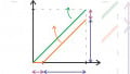
Consider the three-bit characteristic curve shown below (Figure 2).
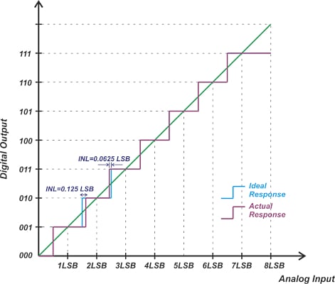
Figure 2. Example of a three-bit characteristic curve.
In this case, only the INL of codes 010 and 011 are non-zero. The largest error occurs at code 010, which can be written in terms of the full-scale value as follows:
\[Error=0.125 \text{ }LSBs=0.125 \times \frac{Full \text{ }Scale}{2^{3}}\]
This can be simplified to:
\[Error=1 \times \frac{Full \text{ }Scale}{2^{6}}\]
Since the conversion error equals the full-scale value divided by 26, we can say its accuracy is 6 bits. What does it mean to have a three-bit ADC with 6-bit accuracy? This means that the error produced by our 3-bit ADC is the same as that produced by a 6-bit ADC with an INL of 1 LSB. In other words, the steps of our ADC are precisely controlled (better than the number of bits of the ADC). As a result, the ADC introduces only a small amount of error beyond its quantization error.
Again, we can use Equation 3 to find the ADC accuracy and get:
\[Accuracy = 3 \text{ }bits - log_{2}(0.125)=3-(-3)=6 \text{ }bits\]
Brief Introduction to Sub-range and Two-step ADCs
Let’s examine the above 3-bit ADC from a slightly different point of view to better understand why an accuracy higher than resolution might be desired.
Assume that we have an ideal three-bit digital-to-analog converter (DAC). We can use this DAC to convert the ADC output back to an analog signal. Subtracting the DAC output from the original analog input, we can find the quantization error (or the “residue” signal) of our 3-bit quantizer. This is illustrated in Figure 3.
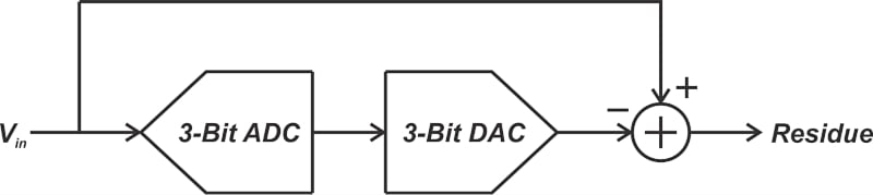
Figure 3. An example diagram showing the "residue" signal from subtracting a DAC output from an ADC input.
Although the ADC has only 3 bits of resolution and introduces a large quantization error, its linearity error is relatively low. With the quantization error being the major error contributor, it’s possible to further process the residue signal through a second ADC to produce an overall resolution higher than 3 bits. This is possible because the linearity error of the 3-bit ADC doesn’t corrupt our signal. We only need to digitize the large quantization error of the 3-bit ADC one more time to achieve an overall ADC with finer resolution. This is actually the principle on which sub-ranging and two-step ADCs operate. A more detailed block diagram of these ADCs is shown in Figure 4.
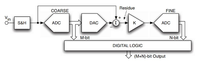
Figure 4. Example block diagram of sub-ranging and two-step ADCs. Image used courtesy of F. Maloberti
The first ADC performs a coarse conversion and determines the M-bit of the most significant bits (MSBs) in the final output. Then the residue signal is processed by a second N-bit ADC. The second stage performs a fine conversion and produces the N-bit LSBs of the output. This structure allows us to trade conversion speed for power consumption and silicon area. For example, a two-step architecture requires a significantly lower number of comparators than a full-flash converter.
With a two-step architecture, the accuracy of the coarse ADC needs to be much better than its resolution. In addition to the coarse ADC, the DAC, and the subtractor also play a key role in the accuracy of the residue signal. That’s why the maximum allowed error of each of these blocks should be determined carefully to achieve a certain overall accuracy performance.
Now that we have established the difference between resolution and accuracy, let’s take a look at a simple example to see how we can calculate the accuracy for an ADC with non-zero offset and gain errors.
Using TUE to Evaluate Accuracy—Non-zero Offset and Gain Errors
Depending on the design goals, one might use either the absolute accuracy or relative accuracy definitions to calculate the “Error” term in Equation 3. A better option that is commonly used in practice is the TUE specification. The maximum TUE can be calculated using the root-sum-square (RSS) of the maximum values of the gain, offset, and INL errors. This can be seen in the equation below:
\[TUE=\sqrt{(Offset \text{ } Error)^2+(Gain \text{ }Error)^2+ INL^2}\]
The RSS method is based on the assumption that the error terms are uncorrelated, and thus, the probability of all error terms being simultaneously at their maximum is small. For example, using this method, we can assume that for a 12-bit ADC, we have:
- INL = 3 LSBs
- Offset error = 2.5 LSBs
- Gain error = 3 LSBs
Assuming that the analog input applied to the ADC can take values in the full input range of the ADC, we can estimate the total error as:
\[TUE=\sqrt{(Offset \text{ } Error)^2+(Gain \text{ }Error)^2+ INL^2}=\sqrt{2.5^2+3^2+3^2}=4.92 \text{ } LSBs\]
Equation 4.
Now, applying Equation 3, we obtain:
\[Accuracy = Resolution -log_{2}(Error)=12-log_{2}(4.92)=9.7 \text{ }bits\]
We sometimes refer to the accuracy obtained from Equation 3 as the “effective number of bits of accuracy.” If we apply calibration to nullify the offset and gain errors, we’ll be left only with the INL error. Note that, in order to use the TUE equation, all of the error terms should be expressed in the same unit (LSBs in the above example).
In practice, the ADC is only one source of error. Several other components (such as the input driver, voltage reference, etc.) can add extra errors and must be considered.
Featured image used courtesy of Adobe Stock
To see a complete list of my articles, please visit this page.


Perhaps I’m getting old, but I’d like to know if there’s still any role for ADC techniques based on voltage-frequency conversion. These were highly developed during the 1990s for isotope ratio measurements, or example in climate studies. Since VFC was commonly used for telemetry, and FM tape recording used to be the only practical way of storing large amounts of analog data, the obvious way to digitise data was to gate the pulses into a counter. You could record either pulses per clock interval, or time to fill the counter.
I have also had to deal with accuracy related to “Best Fit Straight Line”, which was rather tedious to translate into more common terms. That did relate to an encoder rather than an A/D converter, but the information format was the same.
So we have both resolution, very easy to specify and determine, and accuracy, which evidently can be expressed in several different manners. But all are better than the term “precision”, most properly used to describe hardware .
And for the V/F schemes, Our friend, the late Bob Pease was a master at designing and describing them. But they are never as fast as many applications require today.