Facebook
 Google
 GitHub
 Linkedin
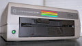
Teardown Tuesday: USB CD Drive
Check out the insides of a USB CD drive in this Teardown Tuesday!
Check out what's inside a USB CD drive.
Even in this age of cloud computing and mp3s, the CD still remains strong as a form of data storage (primarily in the software and games market). However, with the rise of tablets and mobile computing the CD drive is slowly being phased out.
In this teardown, we will look inside a USB CD drive and see how they are made.
The CD Drive Case and Construction
The CD drive shown in this teardown consists of a plastic casing and a USB cable with no buttons for eject or power. It relies entirely on direction from the computer to eject a disk.
The underside of the unit shows a blank plastic mold with no visible screw holes. The edges of the underside show slots that suggest tab fittings. This means a flat object is needed to gain entry.

The CD USB drive

The underside of the CD drive

Tabs on the underside of the CD drive
Removing the lid and base reveals an interesting construction technique with what appears to be a laptop CD drive connected to a custom USB-to-CD-drive converter PCB. The CD drive has all the required products affixed to the topside which includes cautions and safety warnings.

The case removed from the CD drive

The safety and information labeling on the underside of the CD drive

The internal CD-drive-to-USB converter
The USB Converter PCB
The USB converter PCB is connected to the CD drive by using a single socketed connector on the end. The underside of the PCB contains various traces, components, and a crystal while the top side contains ICs and other components. The large number of traces that can be seen on both sides suggests that this PCB is a standard two-layer, FR4 (fiberglass) PCB.

The underside of the USB-to-IDE converter

Underside of the IDE connector

The underside of the USB-to-IDE converter
The top side of the PCB contains two main ICs of interest with the first IC having the identification of INIC-1510L. Online resources show that this IC is a USB-to-IDE bridge which makes this IC responsible for connecting a USB port from a computer to the internal CD drive shown in this teardown. According to initio, the IC contains two bulk endpoints, one interrupt endpoint, DMA controllers, and internal CPU with embedded SRAM and can control hard disks, CDs, DVDs, and removable media devices.

Top side of the USB-to-IDE converter

The initio USB-IDE bridge
The second IC (which is next to the initio USB-IDE bridge IC) has the identification PH25Q40B which makes it a SPI flash memory with a total memory size of 4Mbits. This memory IC may be responsible for holding important information such as device IDs, hardware IDs, and vendor ICs.

The SPI FLASH memory PH25Q
The third IC is a generic 1117 3.3V regulator in an SO-223 package. Even without the ident, its function would be obvious due to the large traces connecting between the IC and the USB input. Since the initio IC uses 3.3V CMOS, the 5V from the USB has to be regulated. Also, since the voltage difference between 5V and 3.3V is small, a linear regulator is ideal (for cost and simplicity reasons).

The power tracks between the 1117 3.3V regulator and USB connector
CD Drive Internals
After removing many small cross head screwdrivers, the top of the CD drive was removed revealing all the internal parts. The centre of the drive shows the motor that spins the CD while the laser assembly can be seen near-by (top right little eye). The drive also includes many levers and springs to push the CD out of the drive upon ejection as well as gear assemblies for various mechanical actions including the stepping of the laser assembly.

Top cover removed showing the internal parts

Motor control for the ejection system

More mechanical actuators
Removal of the many mechanical actuators reveals the PCB, motor, and laser assembly on their own. The PCB is connected to the rest of the drive via flexible connectors which are used to control the motor speed, mechanical parts, and data to and from the laser head. The laser assembly and its associated mechanical controls sit under a metal sheet that protects them from damage and removing this reveals the many different type of gears used. Interestingly, the worm gear that moves the assembly along its rails makes contact with the laser assembly via plastic teeth that are spring loaded as opposed to being fixed. This allows for much greater flexibility and reduces the effort needed to move the assembly along the rails if the rails or any other part should skew or deform slightly.

Metal actuators removed showing the central CD motor and laser assembly

Worm gear used by the laser assembly

Motor and gears used to drive the worm gear
The laser assembly itself is made up of many different parts including optical lenses, laser diodes, and diode detectors. While the exact functions of the individual mirrors and lenses is unknown their global function is to reflect and refract beams coming from the diode and light bouncing off the CD player. This allows for a laser to emit a steady stream of light while a receiver in a different location can receive the reflected signal.

Laser assembly and its optical parts
Main CD Drive PCB
The main PCB in the CD drive is one of the more impressive designs I've yet encountered in a teardown. While it may seem strange, the strong bright colors of the solder mask suggest a thick, high-quality epoxy was used which implies a high-quality PCB.
The topside shows mainly power planes and almost no traces, which suggests that this is at least a four-layer board with the outer layers are being used as an EMC shield. The topside also shows proper PCB routing techniques including the separation of circuit types (with the IC on the left having a separate power plane from the rest of the parts), use of fiducials, proper component legend markings, and large power tracks.

Top side of the PCB that controls the CD drive
On the right side of the PCB is a large IC with the identification of AN22109A but online resources do not suggest what the function of the device actually is. Therefore, its function will have to be determined by deduction! The IC is surrounded by goodness knows how many RC filters and is also near the IDE connector. Considering that there are some other large ICs on the backside of the PCB (more on this later), this IC is possibly a bridge IC that takes data from the CD drive and produces the required IDE signals when requested by an external device.

The first IC, AN22109A
The second IC of interest on the top side of the main PCB has the identification of AN4820 which once again does not yield any results online. However, considering the large 20-ohm resistor nearby, the chunky surface mount capacitor, and its separate ground plane, this IC is probably a motor controller for the eject and spindle.
Analog devices such as motors can be horribly noisy, which is why their ground planes need to be kept separate from high-speed digital circuitry. Another piece of evidence for this assumption is the proximity of the flat flexible cable that goes off to the main motors and other motors on the PCB.

The motor control IC, AN4820
The underside of the PCB reveals three main ICs and various connectors for the flexible cables. Just like the top layer, there are few traces visible which suggests that all the traces are on sub-layers that cannot be seen without destroying the PCB or using an x-ray machine (something that would be fantastic for teardown Tuesday!). The first IC of interest has the identification of MN103SA3GKF which returns nothing of use online with the exception of a single comment describing the IC as an “Interface & Communication IC”. While the function of this IC is not entirely known it can be deduced when looking at the other nearby components.

Underside of the PCB

Main controller, MN103SA3GKF
The second IC of interest is identified as the ESMT M12L16161A, which online resources say is an SDRAM IC.
According to the datasheet, it uses a 3.3V supply, contains 512K x 16bit x 2 banks, and has auto and self-refresh features which make refresh cycles easier to handle.

SDRAM IC, M12L1616
The third IC on the top side has the identification of 29LV400BC which is a FLASH memory device with a capacity of 512K x 8-bit or 256K x 16-bit.
Now that we've identified these other parts, the larger IC (the MN103SA3GKF) can be determined. These other ICs are typically found in computational scenarios and, by looking at the sheer number of pins on the MN103SA3GKF, it can be determined that this IC is the main controller and most likely has a CPU, some internal ROM, and many peripherals to communicate with the other various devices on the PCB.
Data is most likely read in blocks from the CD and directly streamed to the SDRAM thanks to DMA (that also includes the IDE controller IC found on the other side). The main CPU here stores its program in the FLASH memory and uses the RAM for all variables and temporary data storage. Then, when data is ready to be sent out, it will either transmit the data found in the SDRAM to the IDE IC or DMA will allow the IDE controller to directly access the SDRAM. The controller IC, however, will most likely perform tasks such as seeking, writing, reading, and error correction.

FLASH Memory IC, 29LV400BC
Summary
This teardown shows just how incredibly precise modern engineering really is. The drive was not too dissimilar to a Swiss watch with the many spring-loaded internal mechanical actuators and the small gears that make this drive function.
The PCB showed many classic EMC considerations with the segregation of analog and digital parts, the use of multiple layers, ground layers, fiducials, and even tabs for breakout of individual PCBs.
The CD drive product, itself, which was USB-controlled, took a regular internal IDE CD drive and inserted a bridge IC which clearly demonstrates that reinventing the wheel (i.e., designing a USB CD drive from scratch) never pays off and it is better to use off-the-shelf parts!
Next Teardown: Xbox 360 Kinect