 Facebook
 Google
 GitHub
 Linkedin
Teardown Tuesday: Bluetooth Battery Charger
This Teardown Tuesday looks at the Bluetooth LE enabled E4 battery charger by ESyb.
The Esyb E4 4-battery charger has Bluetooth LE for smartphone connectivity. This teardown looks at the components inside the charger.
About the Charger
This Esyb E4 4-battery charger ($32) was purchased by AllAboutCircuits for this teardown. It features Bluetooth connectivity and an LCD screen that provides users feedback about battery state-of-charge and battery type.

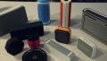
Image of charger and iPhone app from Amazon
Disassembly
Remove the four thermoplastic case screws hidden beneath the rubber pads on the bottom of the case. Then, carefully separate the two halves of the case. Detach the four compression springs from the upper half of the case and remove the two visible thermoplastic screws that secure the circuit board. Carefully lift the circuit board enough to allow you to loosen the flexible flat cable (FFC) and discrete wire connector on the reverse side of the circuit board. Remove the flexible flat cable connected to the circuit board and then lift the circuit board free of the case.
See the video below to watch the teardown.
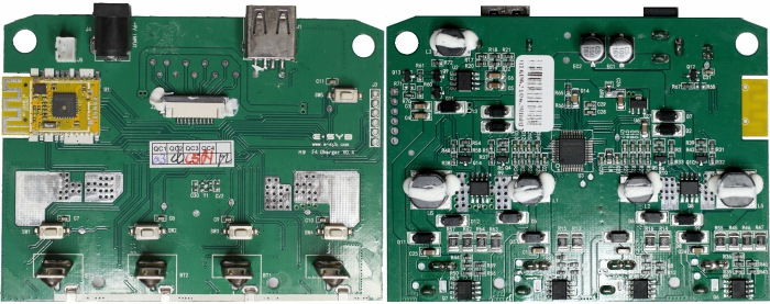
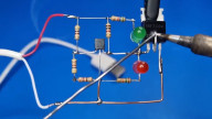
Left: Image of the main circuit board and Bluetooth module. Right: The reverse side of the circuit board.
What's Inside?
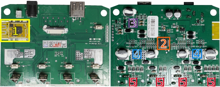
A single internal circuit board holds all charging circuitry and is given Bluetooth communications capabilities with a module based on (1) Texas Instruments CC2541 System on Chip acting as a network processor. A (2) Sinowealth SH88F6161U is the central microprocessor that interfaces with other controller circuitry and the liquid crystal display (LCD not shown). The (3) Chipower CE8421 synchronous boost converter generates power for a USB charge port at the top of the circuit board. The (4) APM4953 and (5) 820862S1G work to charge and monitor individual cells.
| Top-Side Marking | Description | More Information | |
|---|---|---|---|
| 1 | HY-254101 V1 20150807 | Bluetooth 4.0 module | Website |
| 2 | Sinowealth SH88F6161U | Main microcontroller | Data Sheet (cn) |
| 3 | CHIPOWER CE8421 | 5A, 500kHz synchronous boost converter | Datasheet |
| 4 | APM4953 | Dual p-channel enhancement mode MOSFET | Datasheet |
| 5 | 8208 62S1G | AD2808 Precision Differential Amplifier | Datasheet |
(1) HY-254101 V1 BLE Module (Yellow)
This is a Bluetooth low energy module built around the Texas Instruments CC2541 SoC IC. The module holds support circuitry for the chip and a 2.4 GHz antenna.
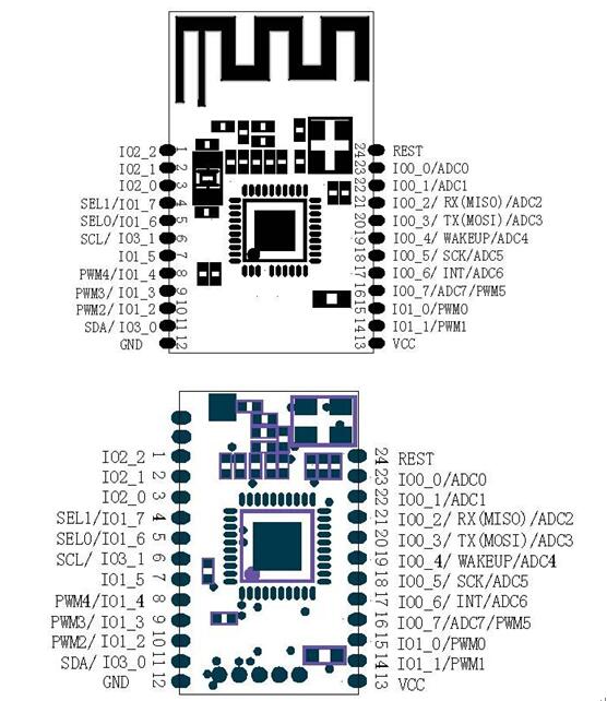
Pinout of the HY-254101 Bluetooth LE Module from manufacturer's datasheet
The CC2541 combines an enhanced 8051 microprocessor with an RF transceiver to create an ultra low power device that communicates with smartphones with the BluetoothLE protocol. With another microcontroller present in the charger, the CC2541 is likely configured as a network processor—a configuration where it remains responsible for wireless data transmission and timing. A network processor configuration communicates with the external MCU via SPI/I²C/UART.
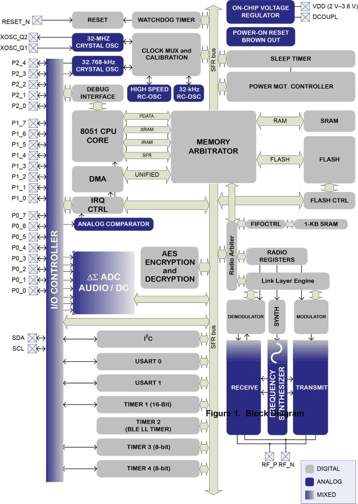
CC2541 block diagram from Texas Instruments CC2541 website
(2) SH88F6161U (Orange)
This enhanced 8051 microcontroller based design has native support for LCD screens as well as all of the standard peripherals that are so common these days: USB, I²C, etc... It is responsible for BluetoothLE communication as well as maintaining the LCD display and controlling the charging circuitry.

(3) CE8421 (Purple)
This 5A, 500KHz synchronous boost converter produces output voltages in the range of 1.8 V to 5.25 V. It is used in this circuit to provide a separate constant voltage source for the USB Type A receptacle at the back of the device.

CE8421 sample circuit from product datasheet
The datasheet indicates that this chip can charge a single-cell Li-Ion or multi-cell NiCd or NiMH battery and its output voltage is controlled with an external resistor-based voltage divider.
(4) APM4953 (Blue)
Each of these two ICs contains two p-channel enhancement-mode MOSFETs located on a perforated part of the circuit board between two inductors and in close proximity to several rectifier diodes. These components are electrically tied to the IC labeled 8208 62S1G (Red, 5) and likely act as support circuitry for these unidentified integrated circuits.
Conclusion
The designers of this circuit managed to squeeze five inductive-based charge circuits and several integrated circuits in close proximity to an unshielded 2.4 GHz BLE transceiver to create an easy to use four battery charger with smartphone connectivity. If any readers out there can identify the component labeled 8208 62S1G, please let us know in the comments below.
Next Teardown: Leeo Wi-Fi Carbon Monoxide and Smoke Alarm


The part marked 820862s1g should be an AD8208 precision diff-amp. Configured as a high side current sense amp for measuring the charge current for each of the 4 cells