 Facebook
 Google
 GitHub
 Linkedin
Teardown Tuesday: Battery Charger
In this teardown, we open up a six-pack sequential battery-charging station, from Milwaukee.
In this teardown, we open up a six-pack sequential battery-charging station, from Milwaukee.
True to its description, this "Six Pack" Sequential Battery Charging Station, by Milwaukee, is designed to charge up to six M18 (18-volt lithium-ion) batteries sequentially.
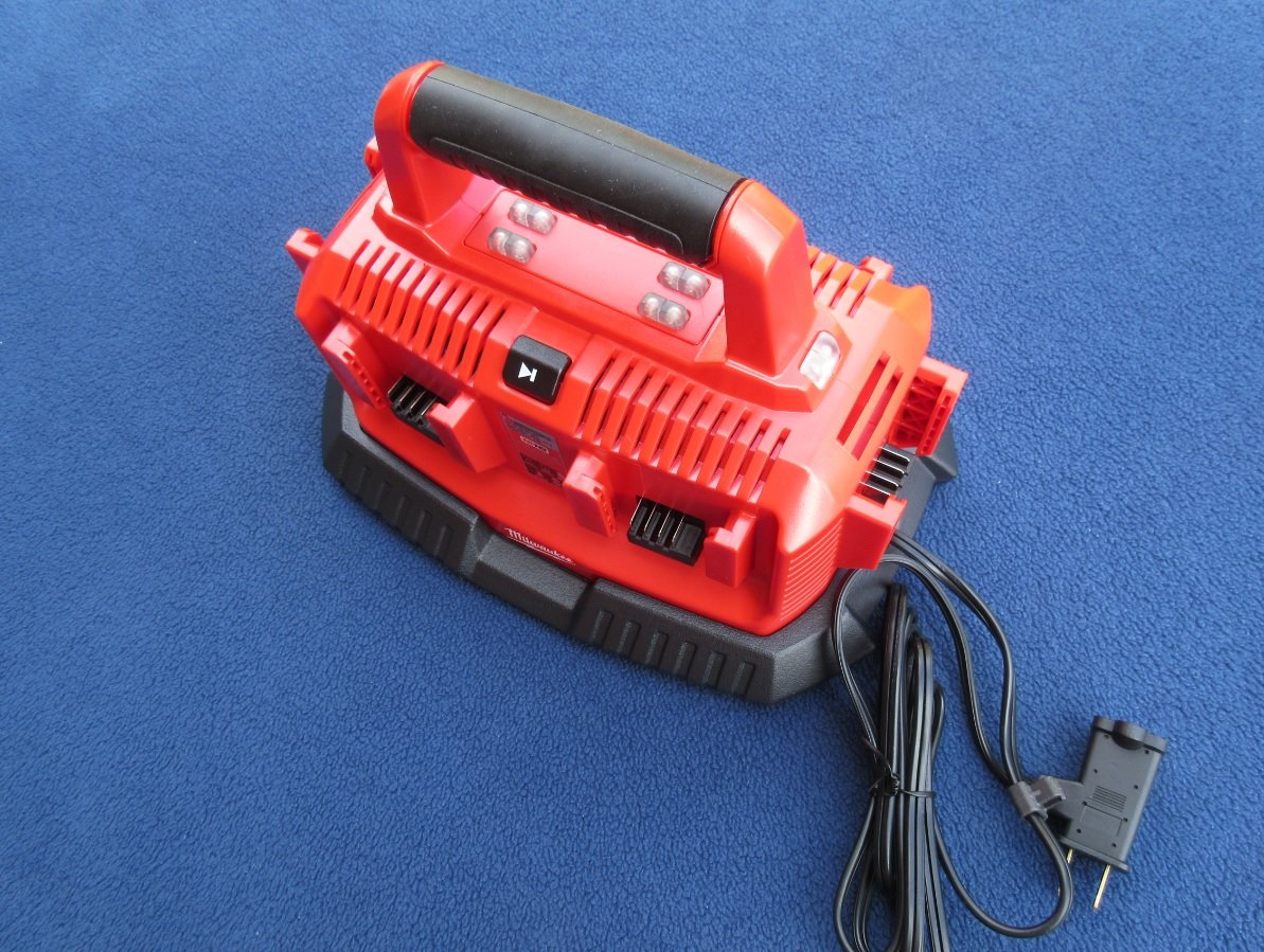
This six-pack battery charging station feels very robust.
Gaining access to this unit's guts was quite the chore because one, it uses Security Torx screws to hold everything together, and two, these special screws are deep down inside the plastic enclosure, meaning that enlarging (i.e., drilling) the holes in the plastic was required. But once the eight or so nuisance screws were removed, I was able to get my first glance at the internal electronics (see figure below).

With the enclosure cracked open, we can see multiple PCBs, wires, and yellow epoxy.
Taking a Closer Look
With the enclosure completely separated (see image below), I noticed that one of the large PCBs was dedicated to managing the high-voltage AC, while the other large PCB handled all the lower DC voltages, as well as the unit's intelligence.
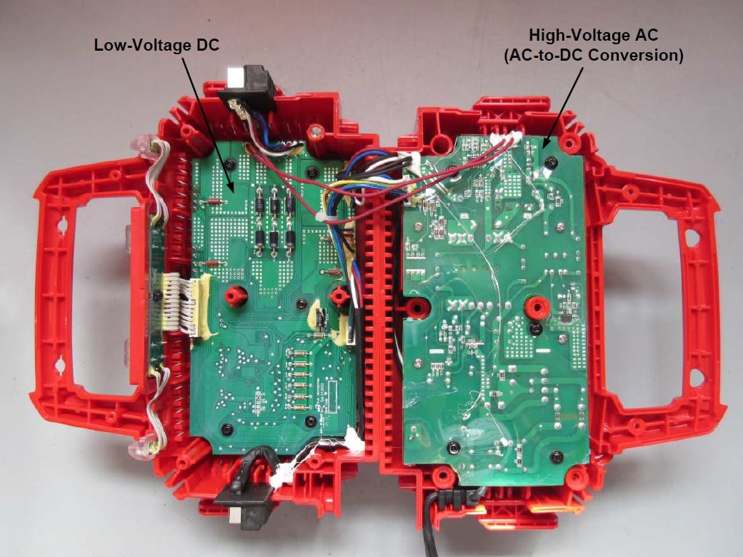
One PCB for AC mains, and one PCB for DC voltage and control.
After removing another fifteen or so Torx screws, the unit's guts could be removed from the enclosure, thus allowing for the inspection and identification of some major components and design insights.
PCBs' Top-Sides
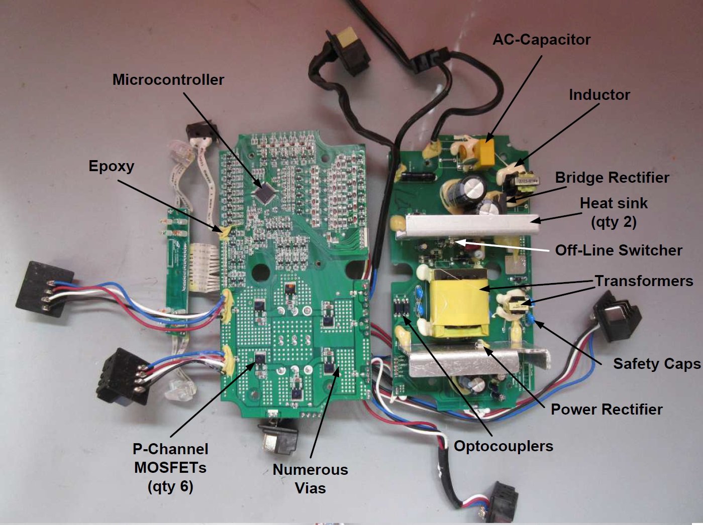
Identifying some of the major components on the PCBs' top-sides.
As can be seen in the above image, this charging station makes use of three PCBs:
- one (on the right side) for managing the incoming high-voltage AC, and converting it to a lower DC voltage;
- one (middle) for directing the lower DC voltage to the desired battery charging port;
- and, a much smaller one (left side) for housing the charging-status LEDs.
All three PCBs are two-layer designs, meaning they have no internal layers. As can be observed, the assemblers used copious amounts of yellow epoxy for securing all the wires and larger components to the PCB; using an adhesive to lock-down wires is a form—although it can be argued to be an inexpensive/cheap method—of strain relief.
Using separate PCBs for high-voltage AC (dangerous voltages) and lower DC voltages (user-touchable voltages) is quite normal. As long as there's adequate distance between the two PCBs, this is a solid design approach for achieving creepage and clearance requirements.
Let's take a closer look at some of the major electrical components on these boards.
PCB: High-Voltage AC
- AC-Capacitor (suppression capacitor): Part marking MKP X2 .47K 300V
- Bridge Rectifier (single phase bridge rectifier): Part marking FL406
- Heat Sinks: These are very robust and thick (approximately 1/8") heat sinks...used to dissipate sizeable amounts of heat.
- Off-Line Switcher: Part marking TOP266EG
- Note: this IC is attached (bolted) to the heat sink.
- Safety Caps: Part marking EG DCF222M Y2 250V. Similar to this part.
- Power Rectifier: Part marking ON Semi BYW29-200
- Note: This IC is also attached (bolted) to the heat sink
- Optocouplers: Part marking 817C
PCB: DC Voltage
While this PCB appears to have a lot going on—meaning, lots of components and copper traces—in reality, most of this PCB contains the same circuits which are merely replicated six times over; each of the six battery ports have their own dedicated circuits.
- Microcontroller: Part marking Microchip PIC16F1946
- P-Channel MOSFETs: Part marking D413A
- Numerous vias: If you notice, this PCB uses many, many vias for the six P-Channel MOSFETs. These vias help dissipate the heat—generated by the MOSFETs—to the copper that resides on both sides of the PCB.
PCB: LEDs
There is nothing fancy about this PCB: it simply contains six LEDs and a few ribbon cable connections, nothing more. I suspect this PCB was extremely inexpensive to design and fabricate. In fact, I'm sure its assembly process, which was obviously done by hand (i.e., not automated), was the most expensive part of this PCB.
PCBs' Bottom-Sides
As can be seen in the image below, the back sides of the PCBs contain very few components. A couple things worth noting:
- Again, we can see the same numerous vias that were discussed in the previous section.
- Wide Trace Gaps: These large gaps, between the AC voltage copper traces, serve to maintain the required high-voltage electrical conductor spacing (see Table 6-1 Electrical Conductor Spacing).
- Diodes: Part marking SB540
- CV/CC Switcher (Constant-voltage switcher with constant-current control): Part marking SC1139DG.
- Operational Amplifiers (quad op-amps): Part marking: AS324AM-E1

The PCBs' back-sides have few components.
Conclusion
This six-pack sequential battery charging station, from Milwaukee, looks (disclosure: I did not actually test this unit prior to tearing it down) to be a well-designed charging unit; the components seem to be rather heavy duty, and there appears to be plenty of heat-sinking capabilities for adequately dissipating the IC-generated heat. If you have any experience using this unit, please share your thoughts on it.
Next Teardown: Space Heater


Wow, thanks for showing this !
I use Milwaukee tools everyday even though I never owned a charging station like this, a friend of mine has one and says it works fine to charge all your batteries overnight since it charges only one at a time therefore not cool if you need a lot of batteries at once.
how can i log into the doctronics.co.uk
cause it is lost