Facebook
 Google
 GitHub
 Linkedin
Build Your Own Clock With Analog Dials, Part 2
We continue our design of a clock that uses analog ammeters to display time and temperature. In this installment, we examine the second of the two circuits that enable the timekeeping function.
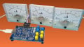
This article is Part 2 of the Analog Clock project. At the end of Part 3, we will have turned three AnalogPAK ICs—Chip A, Chip B, and Chip C—and a trio of microammeters into a working clock that can also display the ambient temperature. The project prototype is shown in Figure 1.
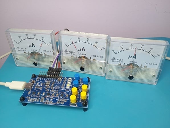
Figure 1. The Analog Clock project prototype.
One microammeter shows the hour, one shows the minute, and one can be toggled to display either the present second or the current temperature. Battery management and multiple backlight modes are also built into the design. A more detailed list of functionalities, along with a full schematic and the project design files, can be found in Part 1.
Part 1 also examines the design of Chip A in detail. Now, in Part 2, we'll do the same for Chip B.
Chip B: Circuit Design and Basic Overview
The design of Chip B is shown in Figure 2. Clicking on the image will open a larger version in a new tab.
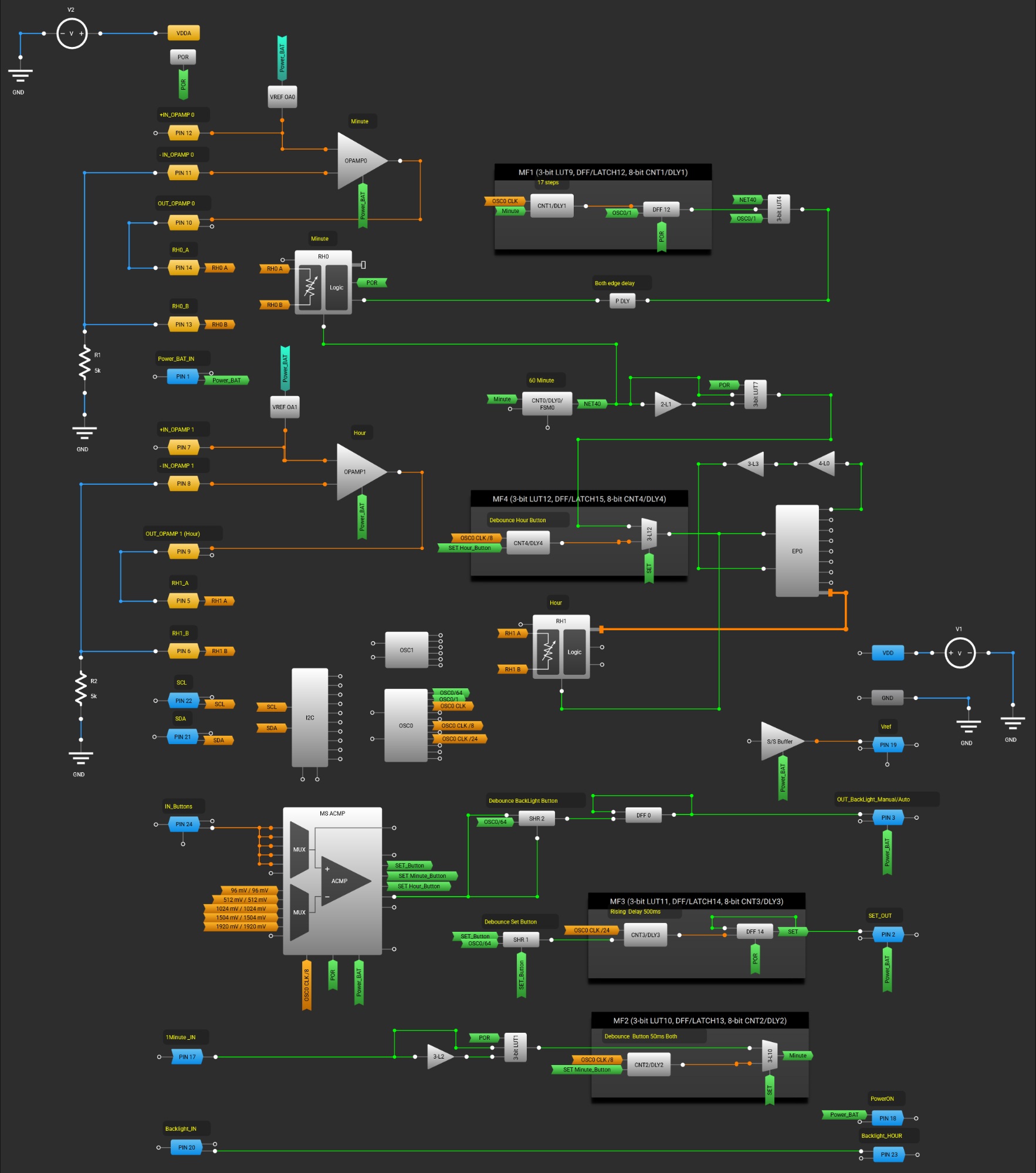
Figure 2. [click to enlarge] Circuit design of Chip B.
As you may recall from Part 1, this IC implements the following:
- Divide-by-60 circuit / minutes counter.
- Minute voltage step generator.
- Divide-by-24 circuit / hours counter.
- Hour voltage step generator.
- Time setting and clock control (clock control button monitoring).
Let's go over each of these.
Divide-by-60 Circuit / Minutes Counter and Minute Voltage Step Generator
The counting of minute pulses and the generation of hour pulses are both performed using an 8-bit CNT0/DLY0, which is configured as a divide-by-60 frequency divider. It follows a similar scheme to the seconds counter in Chip A.
The voltage step generator for minutes is built using OPAMP0, VREF OA0, digital rheostat RH0, 8-bit CNT1/DLY1, DFF12, 3-bit LUT4, and P DLY. It operates similarly to the voltage step generator for seconds in Chip A.
Divide-by-24 Circuit / Hours Counter and Hour Voltage Step Generator
Division by 24 and hour counting are performed using the extended pattern generator (EPG). In this design, the EPG also controls the hour voltage step generator. The digital rheostats are driven by the EPG. In rheostat mode, the 8-bit data from the EPG will be loaded into the activated rheostat counters at the rising edge of the corresponding RELOAD signal.
Figure 3 demonstrates the configuration of the EPG and rheostat RH1. Data corresponding to the resistance values of the digital rheostat RH1 have been added to memory cells 0 through 22. RH1 sequentially accepts these values upon receiving pulses at the CLK EPG input.
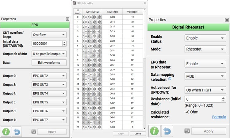
Figure 3. Configuration of the EPG and digital rheostat RH1.
The EPG remains active when a logic-high is present at the nRESET input. The data is selected such that for memory cells 0 through 22, the OUT0 output always holds a logical 1. The signal from OUT0 is fed to the nRESET input through two buffers (3-bit LUT3, 4-bit LUT0). As soon as the EPG reaches Cell 23 (where OUT0 has a logical 0), the EPG is reset to the initial state.
Upon reset, RH1 is loaded with the initial data from the EPG. Subsequent pulses at the CLK EPG input cycle through the memory cells from 0 to 22. The process repeats cyclically with each incoming pulse at CLK EPG. In this way, a single EPG achieves division by 24 and control of the voltage step generator for hours.
The hour voltage step generator in this design is built using OPAMP1, VREF OA1, the digital rheostat RH1, and the EPG. It operates on the same principles as the voltage step generators for minutes and seconds.
Time Setting and Clock Control
To process button presses for clock control—namely SET, Set Minutes, Set Hours, and BackLight Manual/Auto—our design uses the MS ACMP in Range mode. Figure 4 shows the relevant part of the circuit.
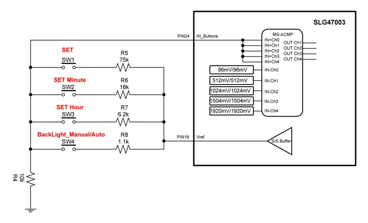
Figure 4. Part of the circuit responsible for processing clock control button presses.
The circuit's operation is based on measuring the voltage across resistor R4. Pressing buttons SW1–SW4 changes the voltage divider ratio based on resistors R5–R8. The dividers are powered by a stable voltage of 2016 mV from the SS Buffer output (PIN19).
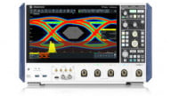
The operating principle of the MS ACMP in Range mode is illustrated by the oscilloscope trace in Figure 5.
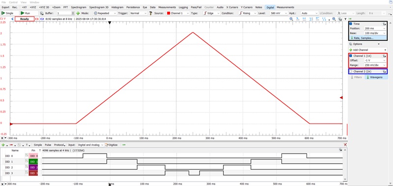
Figure 5. MS ACMP operation in Range mode.
Figure 5 can be read as follows:
- С1 (red) = PIN24 (IN_Buttons)
- DIO 0 = OUT CH1 MS ACMP
- DIO 1 = OUT CH2 MS ACMP
- DIO 2 = OUT CH3 MS ACMP
- DIO 3 = OUT CH4 MS ACMP
The voltage at the IN_Buttons input (PIN24) determines whether a logic-high appears at one of the four MS ACMP outputs listed above (CH1, CH2, CH3, CH4). Table 1 shows the input voltage range that produces a logic-high for each output.
Table 1. A logic-high at each of the four outputs corresponds to a different voltage range.
| IN_Buttons Voltage Range | Logic-High Output |
| 96 mV to 512 mV | CH1 |
| 512 mV to 1024 mV | CH2 |
| 1024 mV to 1504 mV | CH3 |
| 1504 mV to 2016 mV | CH4 |
The four resistor values for R5–R8 are selected such that pressing each button generates a voltage at resistor R4 that falls within the four voltage ranges described above. In this way, we obtain four distinct high-level signals at the MS ACMP outputs. This allows us to process four independent buttons using only one chip pin.
However, due to button contact bounce and the specific behavior of the MS ACMP (during signal rise and fall at the MS ACMP input, other button outputs that were not pressed may also trigger), there is a high risk of incorrect operation of this circuit.
To eliminate the effects of button contact chatter and spurious signals, this design uses debounce filters built on Shift Register 1 (3-bit LUT5), Shift Register 2 (3-bit LUT6), and CNT2/DLY2, CNT4/DLY4.
Figure 6 shows the oscilloscope waveform of signals from the outputs of the debounce filters when pressing the BackLight_Manual/Auto button. As can be seen, false triggering is now absent during the rising portion of the signal.
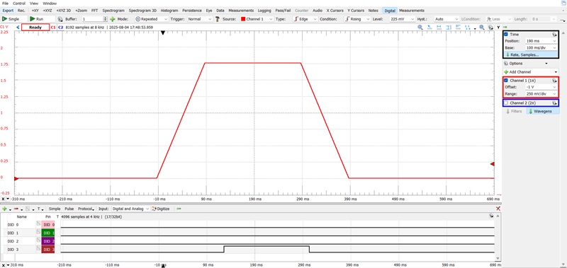
Figure 6. The button-press processing waveform for the BackLight_Manual/Auto button (signals from the outputs of MS ACMP passed through debounce filters).
To interpret Figure 6, note that:
- С1 (red) = PIN24 (IN_Buttons)
- DIO 0 = OUT Shift Register 1
- DIO 1 = OUT CNT2/DLY2
- DIO 2 = OUT CNT4/DLY4
- DIO 3 = OUT Shift Register 2
To eliminate false button triggering, the voltage dividers that generate voltages for each button are powered from a stable source with a voltage of 2016 mV. This voltage is generated using the SS Buffer and VREF.
Multiplexers based on 3-bit LUT10 and 3-bit LUT12 switch signals from the SET Hour_Button, SET Minute_Button, and internal signals from the output of CNY0/DLY0 or PIN 17 (1Minute_IN) according to the control signal SET.
Rising edge detectors are implemented using 3-bit LUT7, 2-bit LUT1, and 3-bit LUT1, 2-bit LUT2. These detectors help eliminate false triggering of the hours counter and EPG during the transition from clock setup mode to normal operation, in cases where the output of CNY0/DLY0 or PIN 17 is at a logic-high.
Up Next
Chips A and B bring the core clock mechanics to life while driving a wonderfully unconventional display. In the final installment of the Analog Clock project, we'll dive into the operation of Chip C. This stage adds some character to the project by handling ambient temperature sensing, the microammeter backlight, and mode switching.
All images used courtesy of Renesas