Facebook
 Google
 GitHub
 Linkedin
Build Your Own Clock With Analog Dials, Part 3
To complete this project, we add backlight control and temperature-sensing functionality to the clock we built in the previous installments.
In Part 1 and Part 2 of the Analog Clock project, we created a compact clock with a microammeter-based display and simple push-button controls. We're now ready to complete the project by incorporating Chip C, which adds the following functionalities:
- Ambient temperature sensing.
- Backlight control for the microammeters.
- Dynamic switching between Temperature and Second display modes.
The design of Chip C is shown in Figure 1. Click on the image to view it in high resolution.
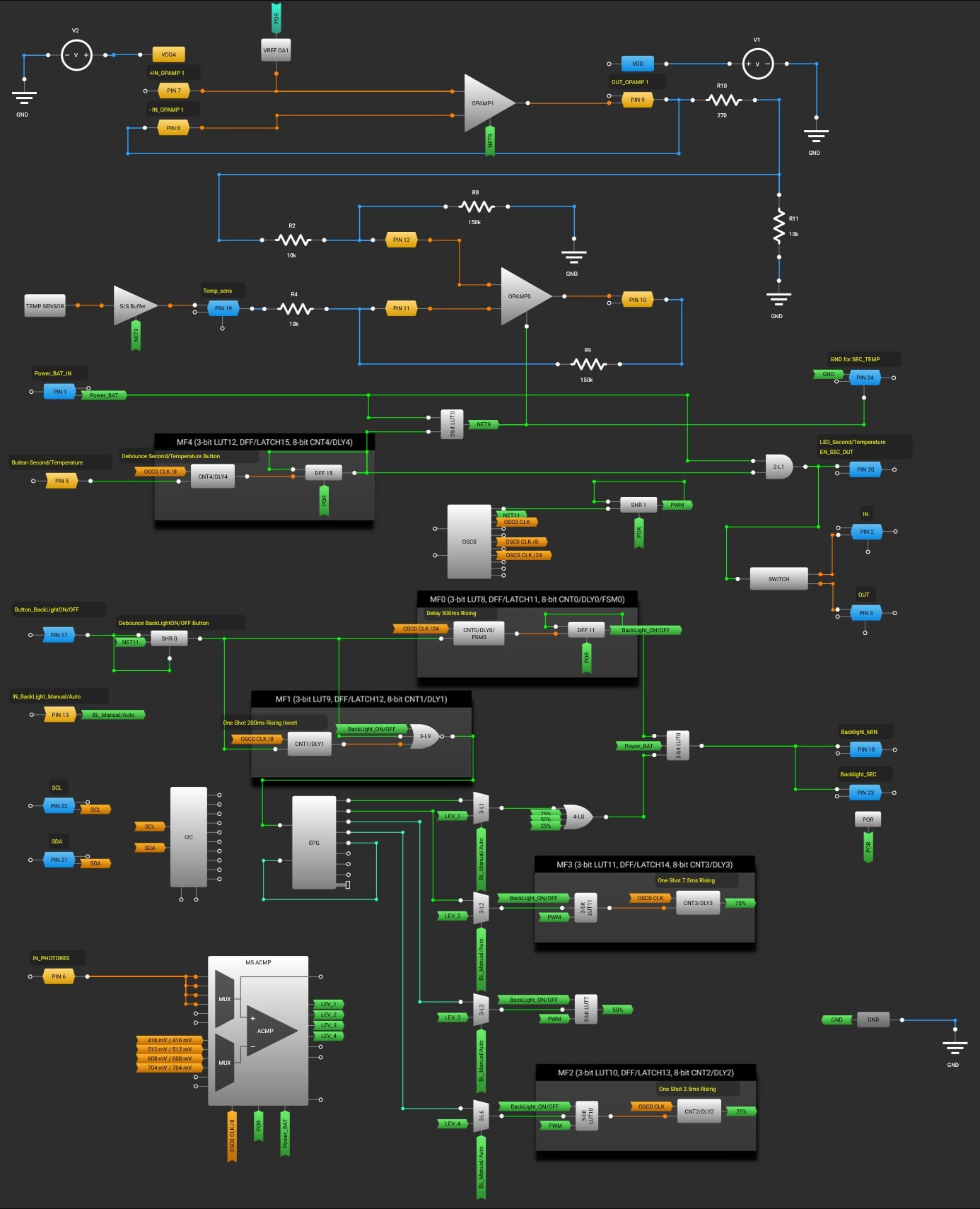
Figure 1. [click to enlarge] Design of Chip C for the Analog Clock.
This design highlights the flexibility of the Renesas AnalogPAK SLG47003, delivering advanced functionality without added circuit complexity or component overhead. Let's consider its operation in more detail.
Temperature Measurement
The following components are used for temperature measurement in this design: TEMP SENSOR, Sink/Source BUFFER, OPAMP0, OPAMP1, and VREF OA1.
The voltage at the TEMP SENSOR output can be calculated using the following formula:
$$V_{TS\text{_}OUT}~=~-4.8~\times~T_J~+~1825.2$$
where:
VTS_OUT = TS_OUT voltage in mV
TJ = Junction temperature in °C.
Thus, for the temperature range from 10 °C to 40 °C, the voltage at the TEMP SENSOR output will vary from approximately 1633 mV to 1777 mV. To achieve a thermometer range of 10 °C to 40 °C and utilize the full display of the microammeter, OPAMP0 is configured as a differential amplifier with a gain factor of 15.
A reference voltage source is built using OPAMP1 and VREF OA1. OPAMP1, configured as a voltage follower, serves to buffer the VREF OA1. The voltage at the output of OPAMP1 sets the starting point of the temperature measurement range (10 °C).
The differential amplifier on OPAMP0 amplifies the difference between a stable reference voltage corresponding to a temperature of 10 °C and the voltage generated at the TEMP SENSOR output. As a result, the output of OPAMP0 provides a voltage ranging from 0 to approximately 2160 mV, which corresponds to a temperature range of 10 °C to 40 °C. The temperature measurement circuit is shown in Figure 2.
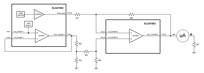
Figure 2. Temperature measurement scheme for the Analog Clock.
The voltage at the output of OPAMP0 can be calculated using the following formula:
$$V_{OUT}~=~\frac{R1}{R6}(V_{+IN}~-~V_{-IN})$$
where:
VOUT = Output voltage OPAMP0
V+IN = +IN input voltage OPAMP0
V–IN = –IN input voltage OPAMP0
R1 = R4
R5 = R6.
Second/Temperature Display Mode Switching
Switching between the Second and Temperature display modes is done using the dedicated button. CNT4/DLY4 functions as a debounce filter for the Second/Temperature button and, together with the configuration of PIN 5 as a digital input with a Schmitt trigger and a pull-down resistor, prevents false triggering due to contact bounce. DFF15 toggles and stores the state of Second or Temperature. 2-bit LUT0 controls the activation of OPAMP0 and changes the state of PIN 24 from LOW to HIGH-Z. 2-bit LUT1 generates the control signal EN_SEC_OUT at PIN 20, and also controls the switch.
Figure 3 shows the control circuit for the microammeter that displays the temperature or seconds value.
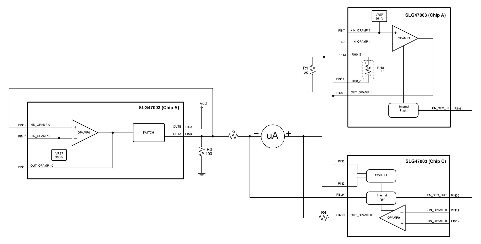
Figure 3. [click to enlarge] Control circuit for the microammeter that indicates temperature and seconds.
In the Second mode, the negative terminal of the microammeter is connected through the current-limiting resistor R2 to PIN 3 of Chip A, while the positive terminal of the microammeter is connected through the closed SWITCH of Chip C to the output of Chip A's OPAMP1. At this time, OPAMP0 of Chip C is turned off by a control signal from 2-bit LUT0, and its output is switched to HIGH-Z, as is the output of PIN 24. This ensures that the temperature measurement circuit does not interfere with the operation of the microammeter and does not affect the seconds display circuit.
Meanwhile, OPAMP1 of Chip A is active, and the microammeter displays the seconds value.
In the Temperature mode, a LOW level appears on PIN 24, connecting the negative terminal of the microammeter to the circuit's GND. The switch opens, disconnecting the output of OPAMP1 of Chip A from the positive terminal of the microammeter, and OPAMP1 of Chip A is also turned off. OPAMP0 of Chip C is activated and connected to the positive terminal of the microammeter through the current-limiting resistor R4. As a result, the microammeter begins to display the temperature value.
Backlight Control
The backlight of the microammeters is turned on by a long press (more than 500 ms) of the BackLight ON/OFF button. It has two modes: manual and automatic. The user toggles between modes by pressing the BackLight_Manual/Auto button.
In manual mode, short presses (less than 200 ms) are used to select one of four brightness levels. In automatic mode, the brightness of the backlight changes depending on the intensity of ambient light falling on the clock. The ambient light intensity is monitored by a light-dependent resistor (LDR).
Shift Register0 functions as a debounce filter for the BackLight ON/OFF button. Together with PIN 17, which is configured as a digital input with Schmitt trigger and a pull-down resistor, it prevents false triggering due to contact bounce. CNT0/DLY0 and DFF11 detect long presses of the BackLight ON/OFF button. CNT1/DLY1 and 3-bit LUT9 detect short presses and block short-press activation in case of a long press.
Adjusting the Backlight Brightness
The brightness is adjusted by changing the duty cycle of the PWM signal controlling the backlight LEDs (100%, 75%, 50%, 25%). The backlight control signal is obtained as follows:
- Shift Register1 is configured to divide the frequency by four. This generates the base PWM signal with a 50% duty cycle.
- PWM signals with 75% and 25% duty cycles are generated from the 50% PWM signal using CNT3/DLY3, 3-bit LUT11, and CNT2/DLY2, 3-bit LUT10.
- 4-bit LUT0 is used to select the desired PWM signal.
A 4-channel 2-to-1 multiplexer is implemented using the elements 3-bit LUT1, 3-bit LUT2, 3-bit LUT3, and 3-bit LUT6. This multiplexer selects the control signal source for the PWM signal generation circuit.
Manual Backlight Control
Switching between PWM signals in manual mode is performed using the EPG. The configuration of the EPG is shown in Figure 4.
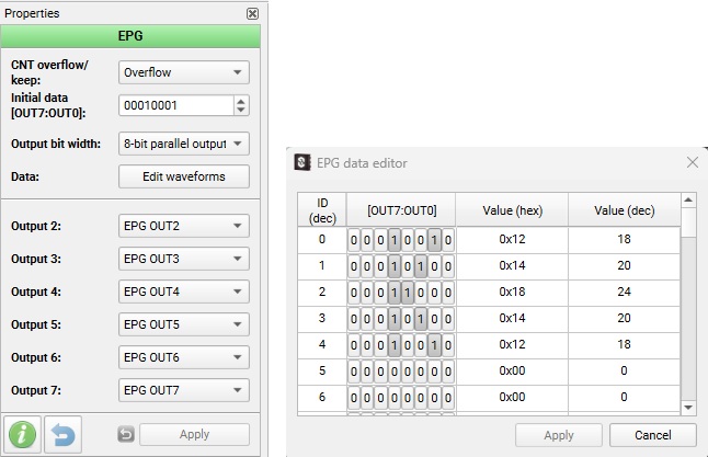
Figure 4. EPG configuration.
This EPG configuration allows the cyclic switching between PWM signals illustrated by Figure 5.
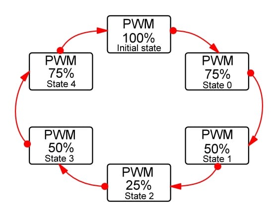
Figure 5. PWM signal switching using the EPG.
The signal from output OUT4 is fed to the nRESET input, and as soon as the EPG reaches state 5 (where OUT4 has a logical 0), the EPG is reset to the initial state. Subsequent pulses at the CLK input of the EPG cycle through states 0 to 4. This process repeats cyclically as pulses continue to arrive at the CLK input.
Figure 6 shows the oscilloscope waveform for the manual brightness control signal.
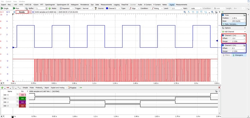
Figure 6. The manual backlight brightness control waveform.
To read this figure, see the following:
- С2 (blue) = PIN17 (Button_BackLightON/OFF)
- С1 (red) = PIN18 (Backlight_MIN)
- DIO 0 = OUT0 EPG
- DIO 1 = OUT1 EPG
- DIO 2 = OUT2 EPG
- DIO 3 = OUT3 EPG
Automatic Backlight Control
In automatic mode, the backlight brightness changes in response to the ambient light. As the ambient light level increases or decreases, so does the brightness of the backlight. As mentioned at the start of the section, the ambient light intensity is monitored by an LDR. The automatic backlight control circuit (Figure 7) is built using the LDR and MS ACMP.
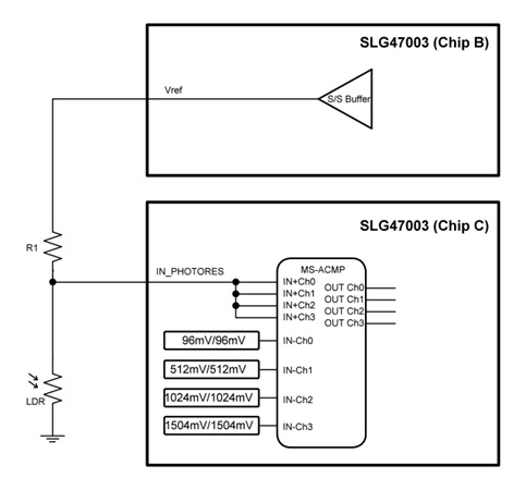
Figure 7. Automatic backlight control circuit.
A voltage divider is formed using R1 and the LDR, powered by a stable reference voltage. The voltage from the divider is fed to the input of MS ACMP. When the ambient light intensity increases, the voltage at the divider decreases; when the ambient light intensity decreases, the voltage increases.
Figure 8 shows the automatic backlight brightness control waveform.
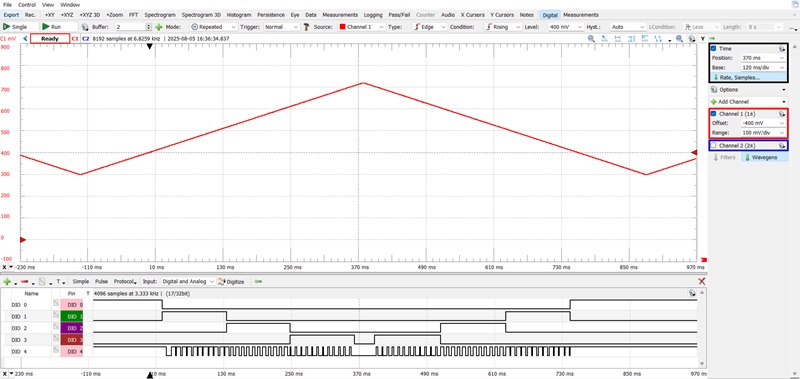
Figure 8. The automatic brightness backlight control waveform.
Figure 8 can be read as follows:
- C1 (red) = PIN6 (IN_PHOTORES)
- DIO 0 = OUT CH0
- DIO 1 = OUT CH1
- DIO 2 = OUT CH2
- DIO 3 = OUT CH3
- DIO 4 = PIN18 (Backlight_MIN)
As an aside, SLG47003V chips feature an I2C module that enables control over a wide range. The use of I2C in this project significantly simplified and accelerated the process of configuration and bug fixing during development.
Operating the Analog Clock
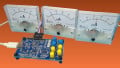
This concludes our discussion of Chip C, the last of the three ICs that make up the Analog Clock. Figure 9 shows the fully assembled project prototype.
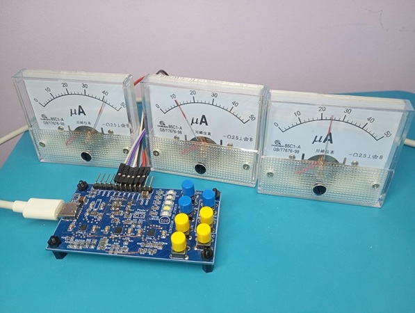
Figure 9. The prototype for the Analog Clock.
To set the time:
- Hold the SET button for ~0.5 seconds to enter time-setting mode (indicated by the SET LED). Note that time-setting mode pauses the seconds counter.
- Use Set Minutes and Set Hours to adjust the time (only incrementing is allowed).
- Use RESET_SEC to reset seconds.
To exit time-setting mode and resume normal operation, hold SET again for ~0.5 seconds.
Wrapping Up
By turning microammeters into dynamic time indicators, the Analog Clock shows how standard components can be used in unconventional ways. Implemented with three SLG47003V devices, it also demonstrates a complete system that brings together analog and digital functions, highlighting how rich functionality can be achieved with minimal external circuitry. I hope you've enjoyed reading about the Analog Clock—now go out and build your own!
Earlier installments of this project can be found at:
Note that Part 1 includes the full Analog Clock schematic and downloadable design files.
All images used courtesy of Renesas