Facebook
 Google
 GitHub
 Linkedin
Build Your Own Clock With Analog Dials, Part 1
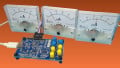
This project turns old-school analog ammeters into a working clock that can also display the ambient temperature.
In a world obsessed with razor-sharp pixels and ultra-bright displays, there's something special about watching an analog indicator move. This project captures some of that retro magic by using AnalogPAK programmable mixed-signal ICs to build a fully functional analog clock. In place of a single clock face, three microammeters team up to tell time: one for hours, one for minutes, and one for seconds. The complete Analog Clock prototype can be seen in Figure 1.
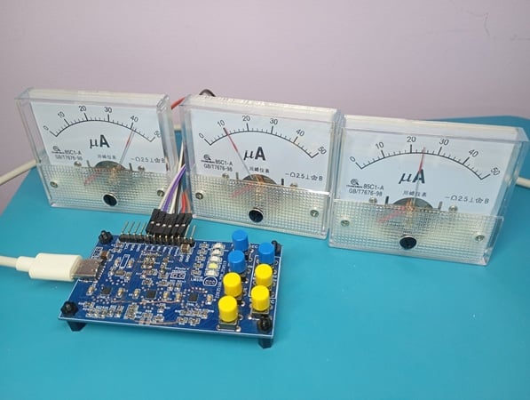
Figure 1. The completed Analog Clock project.
In addition to timekeeping, the Analog Clock also provides the following functionalities:
- Ambient temperature measurement (range: 10 °C to 40 °C), displayed via the analog ammeter normally used for seconds.
- Backlight control for the microammeters. This has both a manual and an automatic mode.
- Battery charging management for the backup power supply.
Crafted in the Go Configure Software Hub, it proves that with a bit of creativity, even the most traditional instruments can get a clever modern twist. Click here to download the design files for this project.
Project Overview and Circuit Design
Figure 2 shows the full Analog Clock schematic. Click on the image to open a high-resolution version.
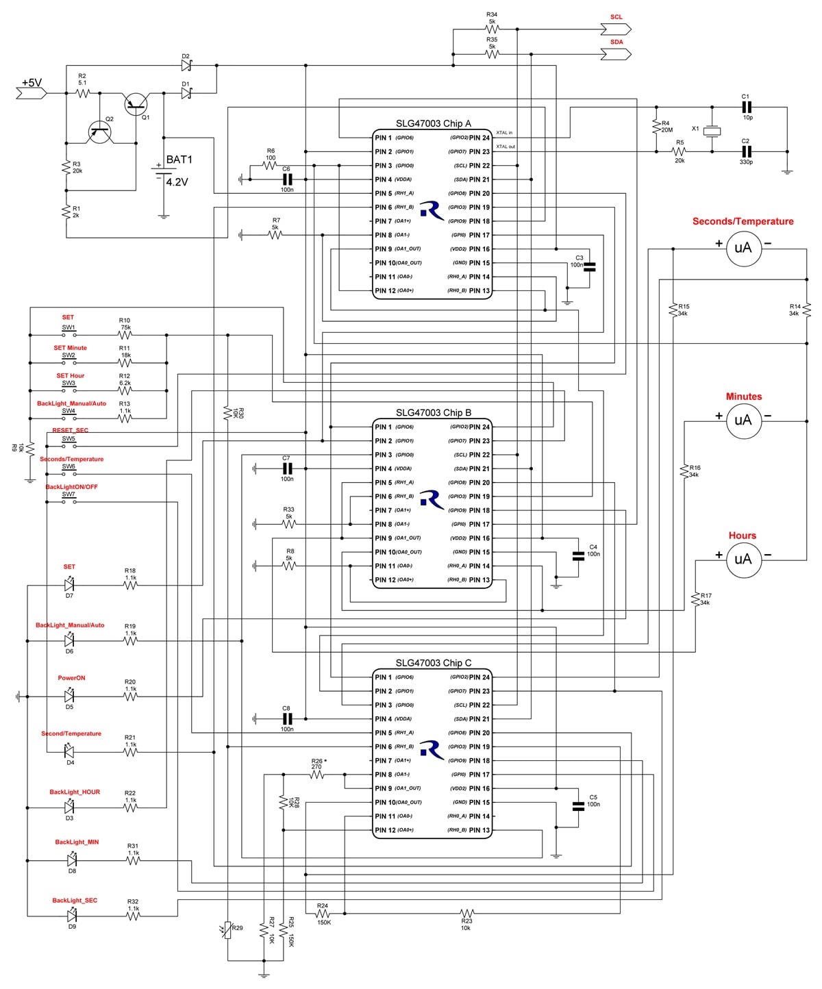
Figure 2. [click to enlarge] Complete schematic for the Analog Clock project.
Chip A implements the following:
- Crystal Oscillator.
- Divider-by-32768/second pulse generator.
- Divide-by-60 circuit / seconds counter.
- Second voltage step generator.
- Time setting and clock control (RESET_SEC, power source control).
Chip B implements the following:
- Divide-by-60 circuit / minutes counter.
- Minute voltage step generator.
- Divide-by-24 circuit / hours counter.
- Hour voltage step generator.
- Time setting and clock control (clock control button monitoring).
Chip C implements the following:
- Temperature measurement.
- Backlight control.
- Switching of the Second/Temperature analog indicator.
All three chips are SLG47003V ICs from Renesas.
Due to space constraints, this project is divided into three parts. Part 1 introduces the Analog Clock project, briefly goes over its design and operation, then focuses on the design of Chip A. Parts 2 and 3 cover Chip B and Chip C, respectively.
Clock Control and User Interface
The clock is operated using seven buttons:
- SET – enters time setting mode.
- Set Minutes – adjusts the minute value.
- Set Hours – adjusts the hour value.
- RESET_SEC – resets the seconds counter.
- Second/Temperature – toggles between time and temperature display.
- BackLight ON/OFF – controls backlight activation.
- BackLight Manual/Auto – switches between manual and automatic backlight modes.
Switching to temperature measurement mode is triggered by a short press of the Second/Temperature button. An LED labeled "Second/Temperature" indicates the active temperature mode.
Brightness Control
The backlight LEDs (BackLight_HOUR, BackLight_MIN, BackLight_SEC) are activated by a long press of the BackLight ON/OFF button. Brightness has four levels and can be adjusted with short presses of the same button.
In automatic mode, brightness adjusts based on ambient light intensity detected by a photoresistor. Switching between manual and automatic modes is done via the BackLight Manual/Auto button.
Powering the Clock
The clock is powered by a 5 V main power source and includes a 4.2 V backup battery. When operating on battery power, the display and backlight are disabled to conserve energy. The PowerON LED indicates main power operation and turns off when the main power is lost.
The clock circuitry also monitors the battery charging voltage and disables charging when the battery reaches 4.2 V.
Design of Chip A for the Analog Clock
Figure 3 shows the design of Chip A. As with the schematic in Figure 2, you can click on the image to view it at full size in a new tab.
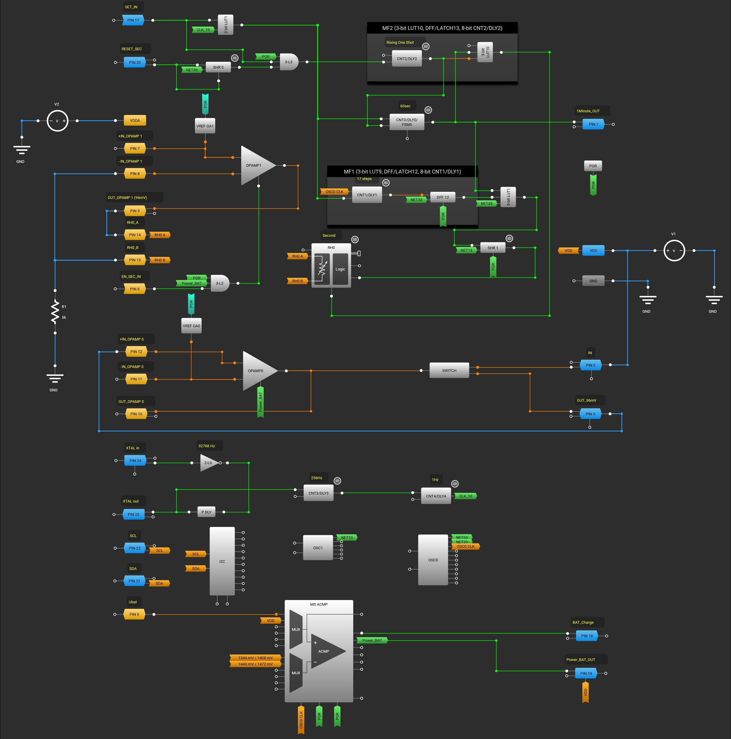
Figure 3. [click to enlarge] Design of Chip A for the Analog Clock
Crystal Oscillator and Divider-by-32768/Second Pulse Generator
The stable pulse generator responsible for generating one-second timing pulses is built using the 2-bit LUT0 (with inverter settings), P DLY, 8-bit CNT3/DLY3 and 8-bit CNT4/DLY4. CNT3 is configured as a divide-by-128 frequency divider, while CNT4 is configured as a divide-by-256 frequency divider. The cascaded connection of the 8-bit CNT3/DLY3 and the 8-bit CNT4/DLY4 results in an overall division ratio of 32,768, thereby generating output pulses with a 1 s period.
Divide-by-60 Circuit / Seconds Counter
The 8‑bit CNT0/DLY0 is configured as a frequency divider with a division ratio of 60.
Second Voltage Step Generator
The voltage step generator in this design is implemented using OPAMP1, VREF OA1, the digital rheostat RH0, the 8‑bit CNT1/DLY1, DFF12, the 3‑bit LUT1, and Shift Register1.
A non‑inverting amplifier is implemented using OPAMP1, whose gain is adjusted by means of the digital rheostat RH0 (Figure 4).
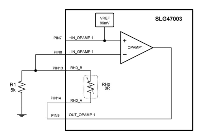
Figure 4. Circuit configuration of OPAMP1 as a step voltage generator.
A stable voltage of 96 mV provided by VREF OA1 is applied to the +IN input of OPAMP1. Thus, OPAMP1 amplifies the input voltage with a gain equal to K. The gain factor is calculated according to the following equation:
$$K~=~1~+~RH0/R1$$
The digital rheostat RH0 has a maximum resistance of approximately 100 kΩ. The minimum resistance is close to 0 Ω. When the resistance of the digital rheostat is varied from 0 to 100 kΩ, the gain of OPAMP1 (assuming R1 = 5 kΩ) changes from 1 to approximately 21. Accordingly, the output voltage of OPAMP1 varies from 96 mV to approximately 2000 mV.
By dividing the entire resistance adjustment range of the digital rheostat into 60 equal steps and increasing the rheostat resistance by 1/60 of its full-scale value each second, a stepwise increasing voltage can be obtained at the output of OPAMP1.
The digital rheostat RH0 provides 1023 switching steps. To utilize the rheostat’s full range, RH0 must be incremented by 17 steps per second. The 8‑bit CNT1/DLY1, DFF12, and the 3‑bit LUT1 are responsible for generating a burst of 17 pulses.
The 8‑bit CNT1/DLY1 generates a pulse with a duration of approximately 1.6 ms on the rising edge of each one‑second pulse. The DFF12 synchronizes this pulse with the OSC0 clock signals. By means of the 3‑bit LUT1, the resulting pulse is filled with 17 clock pulses from OSC0 (see the oscilloscope waveform in Figure 5).
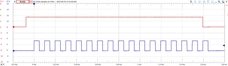
Figure 5. The pulse burst generation circuit waveform. C1 (red) – 8-bit CNT1/DLY1 output; C2 (blue) – 3-bit LUT1 output.
After the resistance of RH0 has increased from 0 to its maximum value, it must be quickly reset back to the minimum. This is done using the Reload input of the RH0 rheostat. The initial value of RH0 is set to 0. CNT0/DLY0 and 3-bit LUT10 generate this signal at the beginning of each minute (when CNT0/DLY0 counts to 60). Shift Register1 introduces a slight delay to the clock pulses for RH0, ensuring that the Reload process completes before the next clock pulses arrive.
At the output of OPAMP1 we receive a cyclic step signal (Figure 6), which can be displayed using an analog microammeter.
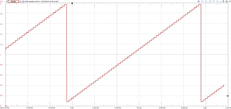
Figure 6. The second's step signal generation circuit waveform.
The step voltage changes from 96 mV, so part of the microammeter scale will not be involved (the arrow will not return to the 0-scale mark). To get rid of this effect, the design uses the circuit on the left side of Figure 7.
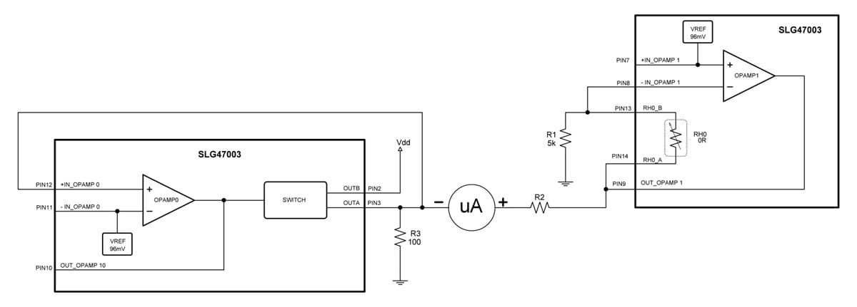
Figure 7. [click to enlarge] Circuit configuration for connecting the microammeter.
This circuit is a voltage stabilizer with an output of 96 mV. Thus, if we turn on the microammeter between the output of this stabilizer and the output of OPAMP1, this will compensate for the offset of the step voltage and the microammeter arrow will return to the zero-scale value.
Time Setting and Clock Control
In this section, we'll discuss the following:
- Processing of button signals.
- Monitoring of power supply voltage levels.
- Monitoring the charge level of the backup battery.
Shift Register0 functions as a debounce filter for the RESET_SEC button. Together with the configuration of PIN 20 as a digital input with Schmitt trigger and a pull-down resistor, this setup ensures protection against false triggering caused by contact bounce.
The elements 3-bit LUT3 and 8-bit CNT2/DLY2 are responsible for resetting the seconds value during time setting. The 2-bit LUT1 blocks the passage of second pulses from the second pulse generator when the clock is in time-setting mode.
MS ACMP monitors the power supply voltage level (Channel 1) and the backup battery charge level (Channel 0).
When Vdd exceeds 4.4 V, MS ACMP outputs a HIGH level on OUT_CH1. This HIGH level keeps the time display active on the clock as long as the supply voltage remains above 4.3 V, which will be the case while the clock is connected to a stationary power source.
Channel 0 of MS ACMP monitors the backup battery voltage level. When the voltage exceeds 4.2 V, it outputs a HIGH level on OUT_CH0. This HIGH level disables the external battery charging circuit and stops the charging process.
Up Next
Now that we've covered Chip A, we'll examine the design of Chip B in Part 2. Together, these two chips are what enable the project's core timekeeping functionality.
All images used courtesy of Renesas