Facebook
 Google
 GitHub
 Linkedin
New Materials Target Interconnect Performance and On-Chip Photonics
New research explores ultra-low-k COF dielectrics, screens topological conductors for nanoscale wires, and reveals high-pressure hexagonal GeSn alloys.
Device scaling is pushing metal lines and dielectric gaps to ever-smaller dimensions, making resistance, capacitance, and material stability first-order constraints.
In recent months, researchers at the University of Houston, Northwestern University, in collaboration with IBM, and the University of Edinburgh have each reported materials advances aimed at different parts of that bottleneck: low-k interlayer dielectrics, nanoscale interconnect conductors, and group-IV alloys for optoelectronic integration.
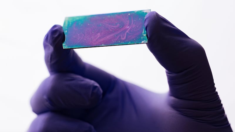
The University of Houston developed a 2D thin-film electric insulator to support faster, lower-power AI. Image used courtesy of the University of Houston
Collectively, these three research efforts show that, alongside the transistor, wiring and the materials surrounding it are increasingly decisive factors in scaling potential.
Rethinking the Dielectric Tradeoff
At the University of Houston, researchers demonstrated large-area, two-dimensional covalent organic framework (COF) films with a reported dielectric constant of approximately 1.17 at 100 kHz. For comparison, conventional organosilicate low-k dielectrics in advanced back-end-of-line processes typically sit well above 2, with porosity used to push values lower at the expense of mechanical strength and breakdown reliability.
 and_doctoral_student_Saurabh_Tiwary_.jpg)
Professor Alamgir Karim (left) and doctoral student Saurabh Tiwary (right) assess the new material. Image used courtesy of the University of Houston
The Houston team, as reported in ACS Nano, synthesized their COF films using liquid-liquid interfacial polymerization, producing thin, continuous layers that were subsequently characterized for electrical and thermo-mechanical performance. In addition to the ultra-low K value, the material exhibited a dielectric strength of about 3,908 MV/m at room temperature and roughly 2,100 MV/m at 300°C. Young’s modulus was measured at approximately 3.4 GPa, with a density near 1.1 g/cm3.
That combination addresses a persistent problem in BEOL integration. Lowering permittivity through increased porosity often degrades breakdown strength and makes films mechanically fragile during chemical mechanical planarization and thermal cycling. The reported COF films aim to reduce capacitance without relying on highly porous structures, while maintaining electrical and thermal stability at elevated temperatures.
The current work focuses on planar test structures, and integration into patterned interconnect stacks will require evaluation under plasma exposure, adhesion to barrier layers, and time-dependent dielectric breakdown testing. Scaling deposition to conformally coat trenches and vias is also an open question. Still, the data suggest that polymer-derived frameworks may offer a different path to sub-2 dielectric constants without the usual reliability penalties.
Screening Conductors Beyond Copper
If capacitance is one side of the RC equation, resistance is the other. As copper line widths shrink down to the few-nanometer scale, surface and grain-boundary scattering drive resistivity sharply upward. This effect has spurred interest in alternative conductors whose transport mechanisms are less sensitive to dimensional confinement.
Northwestern researchers working with IBM reported a computational screening framework to identify topological semi-metals suitable for nanoscale interconnects. Using Wannier tight-binding models and simulations that incorporate surface disorder and roughness, the team evaluated transmission across candidate materials and generated a dataset of roughly 3,000 surface-transport values.
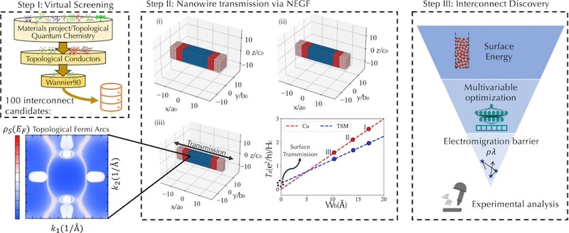
The accelerated topological semi-metal interconnect discovery workflow. Image used courtesy of Advanced Science
The underlying premise here is that certain topological materials host surface states that are robust against backscattering. In sufficiently narrow wires, these surface channels could contribute a significant fraction of the total conductance, mitigating the resistivity inflation observed in copper. Among the materials highlighted were TiS, ZrB₂, and nitrides such as MoN, TaN, and WN, with NbAs and NbP used as benchmarks.
Ultimately, this research establishes a screening methodology and a ranked list of candidates for fabricated interconnect lines based on simulated transport metrics under nanoscale confinement. The next steps will be deposition compatibility, patterning, liner integration, and electromigration characterization. Contact resistance to conventional device layers will also determine whether these materials can realistically displace or complement copper in specific stack layers.
Expanding the Ge–Sn Phase Space
While the Houston and Northwestern efforts target electrical interconnect performance, researchers at the University of Edinburgh addressed the limited phase space of group-IV alloys for optoelectronic applications.
In high-pressure experiments conducted at 9 to 10 GPa and temperatures up to 1,500 K, the Edinburgh team synthesized hexagonal Ge-Sn solid solutions that are not accessible under ambient conditions. The recovered materials adopt a P6₃/mmc structure in 2H, 4H, and 6H polytypes, with hexagonal symmetry observed below approximately 21 at% Sn. Above that threshold, the system reverts to the cubic diamond structure.
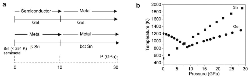
The phase relations of the material (a) and the structural and electronic characteristics of Ge and Sn as a function of pressure and temperature (b). Image used courtesy of the University of Edinburgh
Hexagonal germanium has been reported to exhibit direct bandgap characteristics, though optical transitions can be weak. Incorporating tin expands the lattice and modifies the electronic structure, offering a potential route to tune optical properties within a silicon-compatible materials family. The high-pressure synthesis demonstrates that these phases can be stabilized and recovered at ambient conditions, broadening the compositional possibilities for group-IV semiconductors.
While this work focuses on synthesis and structural characterization, further work will be needed to quantify carrier mobility, optical gain, and defect densities, as well as to explore thin-film growth routes compatible with wafer-scale fabrication. If such materials can be realized in device-ready form, they could support on-chip photonic components without resorting to III-V integration.