 Facebook
 Google
 GitHub
 Linkedin
Teardown Tuesday: Microsoft Xbox 360 Kinect
In this teardown, we inspect the PCBs and their major components (ICs) found inside Microsoft's Xbox 360 Kinect.
In this teardown, we inspect the PCBs and their major components (ICs) found inside Microsoft's Xbox 360 Kinect.
At a Glance
Microsoft's Xbox 360 Kinect is an incredibly smart webcam-like device. It uses an IR (infrared) projector and camera combination to "see" you. Also, it's equipped with a regular (RGB—red, green, blue) color camera so it can film you as well as recognize your face for automatically sign-in for Xbox Live. Its advanced software coupled with the hardware track 48 points of your body in real-time.

Microsoft's Xbox 360 Kinect
Removing the Bottom Cover
Once the bottom cover is removed, a PCB is revealed, along with a cooling fan, a heat sink, and some cables connected to the PCB.
Bottom cover removed
Removing the Top Cover
Removing the top cover allows us to see three PCBs, how they are connected to each other, and how they are connected to the cameras. The three cameras are interfaced to the PCBs using flexible PCBs (also called flex boards), while metal standoffs physically connect the three PCBs together.

Top cover removed
Removing the Parts from the Housing
The image below shows the internal parts and pieces removed from the outer shell/housing.
- The three cameras are solidly secured (screwed) to a metal skeleton.
- The loose cable assembly consists of four microphones.
- The fan is used to force air across the three PCBs for cooling (note that the heatsink has been removed).
- The three PCBs from here on out will be referred to as the "large", "medium", and "small" PCB.
- From a design perspective, it can be assumed that three PCBs were used—as opposed to just one—to minimize the overall volumetric footprint of the product.

The "guts" removed from the housing
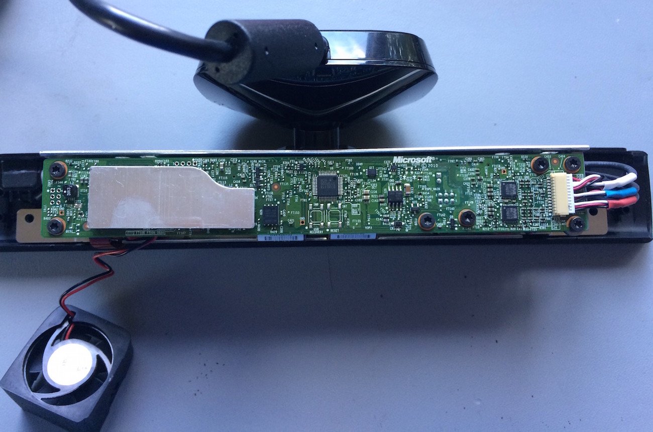
Large PCB (Top-Side)
The major components are called out in the image below.

Large PCB (top-side)
- The holes—with the rather large annular rings—provide proper landing pads and electrical connectivity to the metal standoffs. The vias are used for electrically connecting the top-side of the PCB to its bottom-side.
- This board appears to be a two-sided PCB (i.e., it has no internal layers). This is a great choice for cost savings, although it takes dedicated and focused time and effort on the layout/design team. Well done!
- Samsung DRAM
- Xbox 1101: no datasheet could be found
- NEC D720114: USB hub
- Wolfson Microelectronics WM8737: stereo ADC with microphone preamplifier
- Marvell controller (the brains of the Kinect): no datasheet could be found for this part (Typically, Marvell does not release this information to the public domain.)
- Marvell G39 00A1P: again, no datasheet could be found
Large PCB (Bottom-Side)
The major components are called out in the image below.

Large PCB (bottom-side)
- The board-to-board connectors are used for electrically connecting the multiple PCBs together.
- TI WT245: 4-bit dual-supply bus transceiver
- STMicroelectronics H28A: no datasheet could be found
- Winbond 25Q16BV: 16M-bit serial flash memory with dual and quad SPI
Medium PCB (Top-Side)
The major components are called out in the image below.

Medium PCB (top-side)
- This board also appears to be a two-sided PCB.
- Again, the holes with the large annular rings provide proper landing pads for the metal standoffs
- Analog Devices AD8694: CMOS rail-to-rail output quad op amp
- Allegro A3906: motor driver for the motorized tilt
- Prime Sense PS1080: 3D sensors to provide the image processor and audio/video interface
- Microchip 4LBF: 64k I2C serial EEPROM
- STMicroelectronics (now Micron/Numonyx) M29W800DB: 8-Mbit flash memory
- TI OPA330: 1.8V, 35µA, MicroPower, precision, zero drift CMOS op amp
- TI ADS7830: 8-channel sampling A/D converter with I2C interface
- Microchip 456113: digital POT with non-volatile memory
- Microchip 65471: open-drain output sub-microamp comparators
- Fairchild LVX125: low voltage quad buffer with 3-state outputs
Medium PCB (Bottom-Side)
The major components are called out in the image below.

Medium PCB (bottom-side)
- The PCB-to-ribbon cable connectors are used for attaching the three cameras to the PCB
- Diodes Inc. FZT751: 60V PNP high-performance transistor
Small PCB
The major components are called out in the image below.

Small PCB
- Crystal 6.0000 MHz (unable to locate a datasheet) used by the TI TAS1020B.
- TI TAS1020B: USB streaming controller
- Microchip 464WP: digital POT with non-volatile memory
- Analog Devices ADM706: low-cost microprocessor supervisory circuits
Summary
Microsoft did an excellent job when designing their Xbox 360 Kinect. Given its amazing capabilities, Microsoft designed this product with simplicity in mind. All module components appear to be of high quality and they all attach to each other without the need for too many special tools (though some Torx screwdrivers are required).
I'm a bit surprised to see silk screen on the PCBs. It's common for manufacturers to remove all silk screen from a PCB when a product hits mass-production for two reasons: one is to protect the proprietary information and the other is cost savings. Regardless, the secret sauce of this product lies in the ICs as well as the firmware.
It's obvious that if any parts go bad or otherwise require replacement, they could easily be replaced ... as long as they are available.
Next Teardown: Bluetooth Keyboard


I would like to have the connector reference board to board on the Large PCB (Bottom-Side) please.