 Facebook
 Google
 GitHub
 Linkedin
What Is a Graphene Field Effect Transistor (GFET)? Construction, Benefits, and Challenges
Learn all about graphene field-effect transistors or GFETs. We'll cover their construction, as well as the benefits and challenges of designing with them.
As the size and performance of silicon transistors approach their physical limits, there is a need to look for alternative materials to support emerging technologies. One of these materials being researched is graphene, which is an attractive channel material for field-effect transistors because of its superior electrical, mechanical, and thermal properties.
In this article, we'll talk about the basics of GFETs, including their construction, where they are superior to other field-effect transistors, and where they face challenges.
Defining a Graphene Transistor
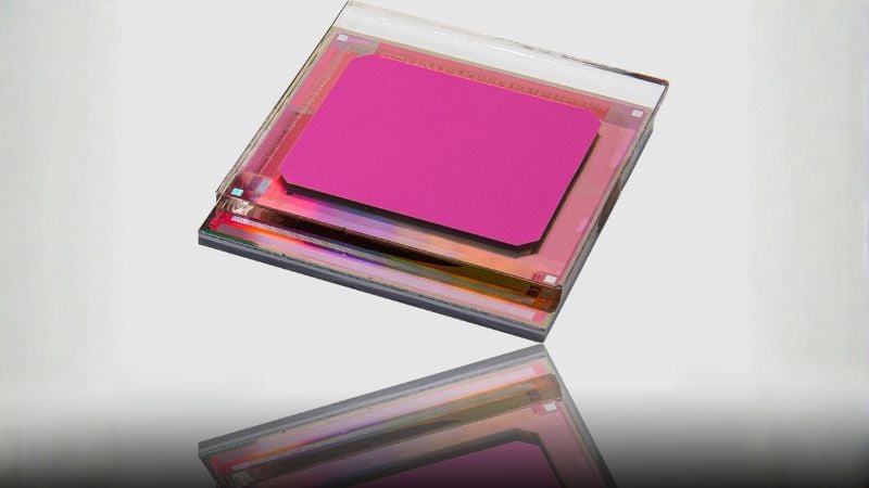
The basic GFET is a three-terminal device that is similar to the conventional FET in some ways. It is composed of a source, drain, and a top or back gate. Unlike a silicon-based transistor, the GFET has a thin graphene channel, usually tens of microns thickness, between the source and drain metal electrodes.

Graphene field-effect transistor with a graphene channel. Image used courtesy of BGT Materials
The gate controls how electrons respond and hence the channel's behavior.
Properties of Graphene Material
Let's talk about the notable properties of graphene material which make GFETs suitable for applications in the electronics, communications, chemical, biological, energy, and other industries.
Graphene is a two-dimensional, single carbon atom layer material which is usually found as tightly-packed atoms in 2D honeycomb or hexagonal lattice.

Structure of a graphene layer. Image used courtesy of CORE-Materials [CC BY-SA 2.0]
Some of the graphene material’s superior properties include:
- High electrical properties: Graphene can theoretically transfer electric current with 100% efficiency. Generally, graphene has a very low resistivity at room temperature, as well as high intrinsic mobility over 100 times that of silicon. Additionally, it exhibits superconductivity under certain conditions (e.g., twisting bilayer graphene at an angle of 1.1 degrees or chilling it to 1.7°C above absolute zero).
- High thermal conductivity: Graphene is an isotropic conductor that dissipates heat in all directions and has better thermal conductivity than other materials, including diamond, carbon nanotubes, and graphite.
- Good optical properties: Graphene is extremely thin, but still visible and can absorb about 2.3% of white light. (which is quite a lot for a 2D material). Combining this ability with superior electrical properties makes graphene an attractive material for building highly efficient solar cells.
- Excellent chemical properties: Graphene is an inert material that does not react with other materials readily. However, under certain conditions, it can absorb some different molecules and atoms that alter its properties. This makes it suitable for applications such as chemical and biological sensors.
GFET Configurations and Gate Bias
There are three main gate configurations for the GFET. Typical transistors can have a top gate, a global back gate, or both, as shown below.
![]()
Different gate configurations in graphene FETs: a) top gate GFET, b) back gate GFET, and c) dual gate GFET
As with traditional silicon FETs, the gate in a GFET controls the flow of electrons or holes across its channel. Since the transistor channel is just one atom thick, all the current flows on its surface, hence the high sensitivity of the graphene FETs.
The current flow in silicon devices is mostly via the electrons or holes. However, the GFET allows equal conduction by both the electrons and holes. Typically, the GFET devices have ambipolar behavior, in which a hole carrier conduction occurs in the channel region under negative bias. On the other hand, a positive bias results in electron carrier conduction.
The two conduction curves meet at the Dirac or charge neutrality point, which should be at zero voltage theoretically. However, in practice, the actual Dirac point may shift depending on doping, the level of impurities on the surface of graphene, the ambient atmosphere, and other conditions. For example, some p-doped graphene FET devices have typical values of 10-40V.
![]()
Transfer characteristics and Dirac point for GFET under a back gate bias
Although the back gate GFET is the most common, the four-terminal GFET that uses both the top and back gates is suitable for some applications. The dual-gate GFET enables biasing the channel with two different voltages.
![]()
Graphene FET dual-gate bias Image from Giubileo, F., & Bartolomeo, A. (2017). The role of contact resistance in graphene field-effect devices. Progress in Surface Science, 92, 143-175.
In typical applications, the dual gated FET uses the two gate biases to control the channel’s charge concentration.
Benefits of Graphene-Based FETs
Graphene's superior electrical and thermal conductivity results in low resistance losses and better heat dissipation than silicon. Consequently, graphene transistors have the potential to provide enhanced performance and efficiency.
The one-atom-thick structure means that the entire channel is on the surface. For sensor applications, the channel is therefore directly exposed to the material or environment under test. As such, some GFETs are highly sensitive and suitable for a wide range of bio- and chemical-sensing applications. For example, it can detect individual molecules detaching from or attaching to a surface.
Finally, researchers have established that using a thin, top-gate insulator material improves GFET parameters such as the open-circuit gain, forward transmission coefficient, and cutoff frequency. Consequently, this opens up other possibilities for GFET applications, including operations at very high frequencies. Theoretically, the transistor has the potential to switch at very high speeds approaching the terahertz range, which is several times faster than what silicon-based FETs can achieve.
The lattice structure of the traditional semiconductor materials has some limitations that cause it to dissipate more heat at higher frequencies. On the other hand, the hexagonal lattice structure of graphene, high electron mobility, and other factors enable it to operate at the terahertz frequencies much better.
GFET Challenges
Graphene FETs are an attractive replacement for silicon-based transistors. However, there are a few challenges that make commercial production difficult, namely:
- Bandgap limitations
- Fabrication costs
- Saturation
Lack of Bandgap
Despite being a fast and efficient transistor, the GFET does not have a bandgap. The gapless structure means that the valence and conduction bands meet at zero volts, hence making graphene to behave like a metal. In semiconductor materials such as silicon, the two bands are separated by a gap which behaves like an insulator under normal conditions.
Usually, the electrons require some additional energy to jump from the valence band to the conduction band. In FETs, a bias voltage enables a current to flow through the band which acts as an insulator in the absence of the bias.
Unfortunately, the absence of a band gap in GFET makes it hard to turn off the transistor since it cannot behave as an insulator. The inability to completely switch it off results in an on/off current ratio of about 5, which is quite low for logic operations. Consequently, using GFETs in digital circuits is a challenge. However, this is not a problem with analog circuits hence making the GFET suitable for amplifiers, mixed-signal circuits, and other analog applications.

E-k diagram for graphene. The enlarged portion shows the zero bandgap at a Dirac point. Image used courtesy of the University of Manchester
Multiple parties are researching ways to address these bandgap challenges, including techniques such as the negative resistance approach and the bottom-up synthesis technique of fabrication.
Delicate and Costly Fabrication
The fabrication process for the graphene transistor differs from that of silicon devices and requires a delicate, complex, and costly method.
The GFET fabrication process involves depositing a graphene layer onto a silicon wafer followed by adding metal contacts at the ends. Manufacturers often use chemical vapor deposition to synthesize the graphene layer. A delamination process then transfers the synthesized graphene and deposits it onto the target SiO2 substrate.
Other steps include constructing the gate dielectrics, gate contacts, and, finally, the contact electrodes using the lift-off process or another suitable method.
Traditional practices often introduce impurities and defects in the graphene channel material. Sometimes this will cause scattering of the charge carriers and degrade the electrical performance in addition to changing the level of doping. Specific problems include Dirac point shifts and low mobility.
Saturation in Analog Circuits
Another challenge in the way of widespread GFET adoption is the insufficient current saturation which prevents the transistor from reaching the maximum voltage gain and oscillation frequency in RF applications.
However, manufacturers can overcome this by optimizing the dielectric material insulating the top gate. Typically, good dielectric gate material provides better control of the carriers in the graphene channel, hence improving performance.
Do you have experience designing with GFETs? What details would you like to learn about GFET implementation? Share your experiences and questions in the comments below.


There’s a much better version of this same technology called a “graphene nanoribbon FET (GNRFET)” which improves on a lot of the issues GFETs have. The downside is that they’re even harder to manufacture.