Facebook
 Google
 GitHub
 Linkedin
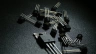
MOSFETS - MOS Field Effect Transistors
Video Lectures created by Tim Feiegenbaum at North Seattle Community College.
In Section 10-3 and we're looking at MOSFETs. MOSFET is an acronym for Metallic-Oxide-Semiconductor Field Effect Transistor. Isn't that a mouthful? A MOSFET is fabricated differently and operates differently than a JFET but it does have some similarities. There are two classes of MOSFETs. There is depletion mode and there is enhancement mode. Each class is available as n- or a p-channel, giving a total of four types of MOSFETs. Depletion mode comes in an N or a P and an enhancement mode comes in an N or a P. We have four different types of MOSFETs.
MOS Field-Effect Transistors: Depletion Mode
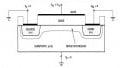
The first one we'll look at is the depletion mode MOSFET. Note, continuous channel of n-type material between the source and the drain. You'll notice here is the source, here is the drain, and we have a continuous channel of n-type material. A voltage placed across the source and drain would induce current flow. We put a voltage in between the source and drain, we would have current flow. The channel acts like a resistor. This is very similar to what we saw in a JFET. Negative voltage will reduce current. We put a negative voltage here, it will tend to increase the resistance of the n-type channel and that would reduce current. A more positive voltage would cause the channel to reduce and resistance and conduct lots of current.
The gate is connected to aluminum which is insulated from the channel by a thin layer of silicone dioxide. Here we have our gate. This is where we differ greatly from a FET is we have actually a metal here. This is aluminum. The aluminum is insulated from the channel by a piece of silicon dioxide. What that's going to do is there's no electrical connection between the gate and the n-type material because we have an insulator in between them, but we will be able to induce an electronic field through the material. There is no connection between the gate and the source and drain.
The three layers led to the device name hence we have Metallic, metallic, oxide, oxide, semiconductors, semiconductors. These three layers led to the device name. Here we have the actual schematic symbol. We have a gate, a drain and a source and is usually connected as three. However, there is an option for a fourth connection and that would be over here. This adds to additional more control. Our main concern is going to be with the three connections.
This is the p-type. This is the same as N except for reversal of the material. The line with the arrow also indicates a connection between the source and the drain right here. Again, the same thing except that materials have been reversed.
Depletion-Mode MOSFET, in a depletion-mode MOSFET, there is a continuous channel or n-type material between the source and drain terminals. With a voltage applied, current can easily flow between the terminals. The metal gate of the MOSFET is insulated from the substrate by a layer of silicon dioxide.
Enhancement-Mode MOSFET
Enhancement-mode MOSFETS, the source, and drain terminals connect to heavily doped n-type silicon in an n-channel enhancement-mode MOSFET. Here we have the source. Here we have the drain. They're connected to heavily doped n-type material. The area between the source and the drain is lightly doped p-type material. There is no continuous channel between the source and the drain like we had with JFETs and with the depletion-mode. Remember, this is enhancement-mode, this is a major difference right here.
A proper polarity gate voltage must be applied for current flow. We're going to need a gate voltage to get current flow and we will address that in a few slides from now. A broken line in the schematic symbol indicates that there is no continuous path from source to drain. When you look at the schematic symbol for an e-mode MOSFET you'll notice that usually, you'd have a continuous line here as we did with FETs and the depletion-mode. Here it is broken and is broken because it is not a continuous channel.
MOSFET Biasing and Operations
The resistance of the channel in a FET depends upon the doping and the physical dimensions of the material. In a MOSFET the effective doping level is modified by the biasing. We're going to look at the biasing in a depletion-mode and an enhancement-mode. We'll start out with the depletion-mode.
If an external DC source is connected between the source and drain of a depletion mode MOSFET, measurable current will flow, notice this, dependent upon the value of the channel resistance. What are we saying? Here we have the source, here we have a drain, and here a voltage is applied through a resistor. We will have current flow through the channel. Now, the amount of current flow will be dependent upon the resistance of the channel. We're going to find that that's going to vary.
By making the gate more positive than the source and increase in source-to-current drain will occur. By making the gate more positive than the source, okay. Here we have our voltage source. There's an interesting thing that takes place in a MOSFET. Notice we have the metallic material right here. It is separated from the n-type material by the insulating silicon dioxide. Then we have the n-type material. Well, this acts as a capacitance. The silicon dioxide in effect is the dielectric material and the metal here is one side of the capacitor and the n-type material is the other side. As we apply a positive voltage here, what will occur is that we'll have a positive charge on this side. We will have a negative on this side. The negative here will represent free electrons and this will take that n-type material adding many more free electrons. It will be heavily doped n-type material and it will easily conduct current flow and it will have very little resistance to current flow.
In the second scenario, if the gate is made more negative than the source, the channel doping is effectively reduced slowing current flow. This picture is the same as this except that we have changed the biasing on the gate. Now, we're putting a negative voltage on the gate. We're having that same capacitance effect except that now the electrons are on the top plate. We have a positive charge on the bottom. This effectively reduces the doping level in the n-type material. Depending on the amount of negative voltage, this will become extremely resistive and it will impede current flow.
In the depletion-mode MOSFET, the charge on this capacitor ultimately determines how much current is going to flow through the channel. Now, in an enhancement-mode MOSFET, when a positive gate voltage is applied, the gate capacitance charges to the value of the gate-source voltage. Now remember, actually in this drawing here, this n-type material is not continuous, it's kind of like this right here. Again, we're placing the positive voltage. Again, there is that capacitance phenomenon. Here we have the positive charge on the top plate if this is a positive voltage. Then we have a negative charge. The negative charge here is not in the p-type material. Actually, the negative charge is right along the edge of the silicon dioxide. What this forms is what's referred to as an n-type inversion layer. It's not truly n-type material but it's referred to as an n-type inversion layer. This thin layer is right along the edge of the silicon and it will be heavily electrons. What will end up happening is that this will cause current to flow along the edge of that silicon dioxide and we will have current flow. That is with a positive voltage on the gate.
When we do just the opposite, again, this is the same thing except that now we have a negative voltage here. The capacitance, again, the charge, the negative, the electrons will be on top. The positive charge will be along the bottom. This will effectively cut off currently flow. There'll be no current flow because there is no path at this point. There's no n-type inversion layer so we have this positive and the p-type material and we will cut off current flow. Now there is an incomplete channel and it will be cut off.
This has introduced the depletion-mode and enhancement-mode MOSFET devices. We've also looked at the biasing of both devices.
Related Content