Facebook
 Google
 GitHub
 Linkedin
Bipolar Transistors (intro)
Video Lectures created by Tim Feiegenbaum at North Seattle Community College.
We're into Chapter 10. We're looking at transistors and transistor circuits. Transistors gained widespread usage in the early 1960s, replacing vacuum tubes in electronic circuits. Over here to the right, we see a picture. This was actually the first transistor. It was invented in 1948 and you notice this large bulky size here. It would be miniaturized dramatically over the years and it was actually invented at Bell Labs.
They replaced the vacuum tube prior to the transistor. All electronic circuits were built using large bulky vacuum tubes and it is severely restricted, electronic development, just because of the size. Transistors were responsible for making components much smaller and they led to the information age, actually.
Today, the integrated circuit has replaced discrete components like the transistor. Because integrated circuits are designed around discrete components like transistors, it is essential to have an understanding of transistor operations. The main reason that we're looking at transistors is because transistors are foundational to understanding integrated circuits. Today, we primarily use integrated circuits which are literally millions of transistors etched on with a piece of silicon. To understand how this works, you need to have at least a grasp of how this transistor works.
Now, before I leave this, I will say that there are many circuits today that still utilize transistors but much of their use now has been integrated into much smaller components.
Bipolar Transistors
The diodes discussed earlier are bipolar devices as their operation depends upon holes and electrons as current carriers. Two additional bipolar devices are the NPN and the PNP and these are bipolar transistors. Now, we will look at something called the unipolar transistor later in this chapter, but for now, we're going to focus on bipolar transistors.
Construction
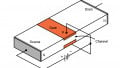
NPN transistors consist of three layers of semiconductor material, okay? Three layers and they make up a thin layer of p-type material sandwiched between the regions of N-type material. Here we have the three regions here and this p-material is sandwiched in between the two pieces of N-material. This is probably shown bigger than it really is. The p-material is really quite very thin. Two PN junctions are formed as a result so you have a PN-junction from here to here and another PN junction from here to here.
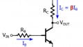
A lead is attached to each of these three regions so we had a lead attached here, here, and here and this makes up the emitter, the base, and the collector. This is the schematic symbol that you would see in a transistor. Keep note. The arrow is always pointing to the N-material, so in this case, this is n. The base would have to be p so that would be an NPN transistor.
Okay, let's talk a little bit about the makeup of this. Notice the emitter, there's a note here that is heavily doped and so when we talked about heavily doped n-material, that means that it's doped so that it will have an excess of electrons. I'll put many dots in here indicating that this is very heavily doped. Now, the p-material--notice it is very thin and it is lightly doped, in this instance, p-material. We'll have a few holes in here, but as p-material goes, it is light doped. It has very few carriers inside it. Then we have the collector and it was moderately doped so we're going to see that it has electrons but not nearly as many as we would see in the emitter. This is the NPN transistor and I just emphasize the fact that the base is very thin and it is very lightly doped. We'll see that becomes crucial in the operation and the transistor later.
Okay, PNP transistors. They are complements of NPN transistors and you'll notice here a set of--NPN now is PNP. The schematic symbol remains the same except that notice the arrow, again, was pointing at the base since the base is n-material. Now, we would have this configuration PNP. It's very important to look at where is the arrow pointing when you look at a transistor to determine what kind that is.
Again, the same relationships exist. The emitter is heavily doped. Only this time it would be heavily doped, but since this P-material it would be heavily doped with holes. The base is lightly doped so it would have a few electrons and the collector is lightly doped. It would have just a few holes. Again, a very similar relationship and notice that this is a complement of NPN. In actual usage, you're probably going to see more of the NPN. The PNP is going to require a little bit different voltage arrangement on, typically. The biasing is different and most of our focus will be on NPN.
Okay, that completes our introduction to transistors so we looked at PNP and we looked at NPN, and we have emphasized the fact that the emitter is heavily doped, base lightly doped, and the collector moderately doped. Please recall that the arrow will always point at the n-material.
Okay, that concludes our introduction to the bipolar transistor.
Related Content