 Facebook
 Google
 GitHub
 Linkedin
Bipolar Junction and Field Effect Transistors (BJTs and FETs)
The word “transistor” refers to a semiconductor device that can perform switching and amplification. As you might recall from a previous tutorial, an electronic device that can function as a switch or an amplifier is called an active component. Electrical switching and amplification did not begin with the invention of the transistor in 1948; however, this invention was the beginning of a new era, because transistors were small, efficient, and mechanically resilient compared to the active components—called vacuum tubes—that were used prior to the proliferation of transistors.
This video tutorial will briefly discuss the basic characteristics and functionality of the two most common types of transistors. Later in this course, we’ll learn more about how transistors operate and how they are used by circuit designers.
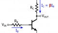
The Bipolar Junction Transistor
In the previous tutorial we learned about the special characteristics of a pn junction. If we add one more section of semiconductor material to a pn junction, we have a bipolar junction transistor (BJT). As shown in the following diagram, we can add a section of n-type semiconductor to create an npn transistor, or we can add a section of p-type semiconductor to form a pnp transistor.
![]()
A three-layer combination of n-type and p-type semiconductor results in a three-terminal device that allows a small current flowing through the base terminal to regulate a larger current flowing between the emitter and collector terminals. In an npn transistor, the controlling current flows from the base to the emitter, and the regulated current flows from the collector to the emitter. In a pnp transistor, the controlling current flows from the emitter to the base, and the regulated current flows from the emitter to the collector. These current patterns are conveyed by the arrows in the next diagram.
![]()
The Field-Effect Transistor
As the name implies, a field-effect transistor (FET) uses an electric field to regulate current. Thus, we can think of the BJT and the FET as two fundamental variations on the theme of semiconductor amplification and switching: a BJT allows a small current to regulate a large current, and an FET allows a small voltage to regulate a large current.
A field-effect transistor consists of two doped semiconductor regions that are separated by a channel, and a voltage is applied to the device in such a way as to alter the current-carrying properties of the channel. The diagram below gives you an idea of how this works.
![]()
As you can see, the terminals separated by the channel are called the source and the drain, and the gate is the terminal to which the controlling voltage is applied. Though this diagram helps to introduce general FET operation, it is actually depicting a relatively uncommon device called a junction field-effect transistor (JFET). Nowadays, the vast majority of field-effect transistors are metal oxide semiconductor field-effect transistors (MOSFETs).
A MOSFET has an insulating layer that separates the gate from the channel. Thus, unlike a BJT, a MOSFET does not require steady-state input current; the current flowing through the channel can be regulated simply by applying a voltage. The following diagram conveys the physical structure and basic operation of an n-channel MOSFET, also called an NMOS transistor. The majority carriers in an NMOS transistor are electrons; the p-type version, which has holes as majority carriers, is called a p-channel MOSFET or PMOS transistor.
![]()
Two heavily doped n-type regions are separated by a p-type channel. Let’s assume that the source and the substrate are connected to ground. If the gate is also grounded, current cannot flow through the channel because a voltage applied to the drain results in a reverse-biased pn junction. However, a positive voltage applied to the gate repels holes in the channel, thus creating a depletion region, and attracts electrons from the source and drain sections. If the voltage is sufficiently high, the channel will have enough mobile electrons to allow current to flow from drain to source when a voltage is applied to the drain.
Conclusion
Because they allow a small current or voltage to regulate current flow, BJTs and MOSFETs can function as electronic switches and amplifiers. Switching action is accomplished by supplying an input signal that transitions between two states; one of these input states results in full current flow, and the other results in zero current flow. Amplification is accomplished by biasing the transistor such that small input-signal variations create corresponding larger-amplitude variations in current flow.
Transistors can be manufactured as discrete devices, but they are most frequently encountered as tiny components within integrated circuits, and these integrated circuits are what we will study in the next chapter.
Related Content


It is a good concept i do appreciate the proveders.
Woow, good like 👌
Good!