 Facebook
 Google
 GitHub
 Linkedin
The PN Junction Diode and Diode Characteristics
Semiconductor components—not only diodes and transistors but also less-common devices such as TRIACs and silicon-controlled switches—are constructed by combining n-type and p-type semiconductors. Thus, it is important to understand what occurs at the interface between n-type and p-type materials; we call this interface the pn junction.
The pn Junction and the Semiconductor Diode
When we’re focusing on the physics of semiconductor operation, we use the term pn junction; when we’re focusing on circuit design, we use the term diode. But they’re essentially the same thing: a basic semiconductor diode is a pn junction with conductive terminals attached.
First, let’s look at a diagram, and then we’ll briefly explore the behavior of this extremely important circuit element.
The unfilled circles on the left are holes, and the solid circles on the right are electrons.
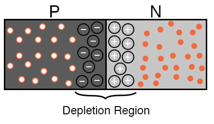
The depletion region consists of holes that have recombined with free electrons from the n-type semiconductor (these recombined holes are represented by circled negative signs) and electrons that have recombined with holes from the p-type semiconductor (represented by circled positive signs). This recombination causes the p-type portion of the depletion region to be negatively charged and the n-type portion of the depletion region to be positively charged.
The separation of charge at the junction of the p-type and n-type materials results in a potential difference called the contact potential. In a silicon pn-junction diode, the contact potential is about 0.6 V. As you can see in the previous diagram, the polarity of this potential is the opposite of what we might expect: it is positive on the n-type side and negative on the p-type side.
Current can flow through the junction by means of diffusion—because of differences in charge-carrier concentrations in the two portions of the junction, some holes from the p-type material will diffuse into the n-type material, and some electrons from the n-type material will diffuse into the p-type material.
However, very little current flows because the contact potential functions as a barrier to this diffusion current. At this point we will begin using the term barrier voltage instead of contact potential.
Forward and Reverse Bias
If we connect the diode to a battery such that the battery’s voltage has the same polarity as the barrier voltage, the junction is reverse-biased. Diffusion current is further impeded because we are increasing the barrier voltage.
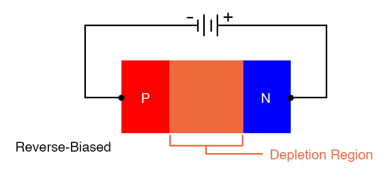
Applying a reverse-bias voltage widens the junction’s depletion region.
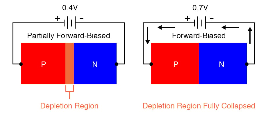
If, on the other hand, we connect the battery’s positive terminal to the p-type side of the diode and the negative terminal to the n-type side, we are decreasing the barrier voltage and thereby facilitating charge-carrier diffusion across the junction.
However, the amount of current will remain quite low until we overcome the barrier voltage and fully collapse the depletion region. This occurs when the applied voltage is equal to the barrier voltage, and under these forward-biased conditions, current begins to flow freely through the diode.
Diodes as Circuit Components
The preceding discussion reveals the underlying physical processes that produce the two most prominent characteristics of a silicon diode’s electrical behavior.
First, a pn junction resists current flow when voltage is applied in reverse-bias polarity and allows current flow when voltage is applied in forward-bias polarity. This is why a diode can function as a one-way valve for electric current.
Second, current flow through a diode increases exponentially as the applied forward-bias voltage approaches the barrier voltage. This exponential voltage-current relationship causes the voltage drop of a forward-biased diode to remain fairly stable, as conveyed by the following plot.
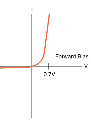
Diode operation can be approximated as a constant voltage drop because large increases in current correspond to very small increases in voltage.
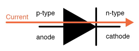
The following diagram clarifies the relationship between the physical structure of a diode, its circuit symbol, and the names that we use for its two terminals. Applying a forward-bias voltage causes current to flow in the direction of the orange arrow.
Conclusion
We have now covered foundational aspects of semiconductor functionality, and in the next tutorial, we’ll explore the transistor, which is the semiconductor component that ushered in the electronic age.


Common on, in the diagram just above the heading “Diodes as Circuit Components”, the symbols for batteries are inconsistent with the polarity indicators (’+’, ‘-’). It confused me!