Facebook
 Google
 GitHub
 Linkedin
Semiconductor Basics: Materials and Devices
In this video tutorial, we'll discuss semiconductor materials and how they become useful electronic components—namely, through semiconductor doping.
What Is a Semiconductor?
The word “semiconductor” has become associated with the sophisticated electronic technology that rapidly transformed human life during the second half of the twentieth century. However, on its own, a semiconductor is rather unremarkable: it is simply a material that exhibits mediocre conductivity—that is, it’s less conductive than a conductor but more conductive than an insulator.
Thermal energy causes valence electrons to break out of a semiconductor’s lattice structure and thereby become “free” electrons. These mobile electrons are negative charges that can move under the influence of an applied electric field, and the holes left behind by these free electrons function as mobile positive charges. Both electrons and holes participate in semiconductor current flow, and the electrical properties of a semiconductor are affected by the number of free electrons and holes that are present in the material.

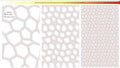
The diagram on the left represents the regular crystal lattice of a semiconductor, and the diagram on the right includes an electron-hole pair.
Ordinary unmodified semiconductors don’t offer much in the way of useful electrical functionality. The first step in turning a semiconductor into a means of technological revolution is called doping.
Semiconductor Doping
We can control the quantity of charge carriers in a semiconductor by injecting other materials into the lattice structure. More specifically, we inject materials that have a different number of valence electrons.
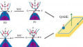
Let’s say that our semiconductor is silicon (Si), which is a group IV element and thus has four valence electrons. As shown in the previous diagram, silicon atoms combine via covalent bonding into a regular lattice structure. A group V element such as phosphorus (P) has five valence electrons, and if we inject phosphorus into the silicon, each injected atom will introduce a free electron into the semiconductor’s crystal lattice:

Doping with a group V element introduces free electrons.
In this situation, phosphorus functions as a dopant and the silicon becomes an n-type semiconductor: it has received additional free electrons through doping, and when an electric field is applied, current flow will be due primarily to electrons, which have a negative charge. Thus, in an n-type semiconductor, electrons are the majority carriers and holes are the minority carriers.
If, on the other hand, we dope with a group III element such as boron (B), each doping atom will introduce an additional hole. This turns the silicon into a p-type semiconductor: holes outnumber free electrons, and current flow will be due primarily to the movement of positive charges. Thus, in a p-type semiconductor, holes are the majority carriers and electrons are the minority carriers.

Doping with a group III element introduces holes.
The injected element is not the only variable in doping procedures. We can also control the dopant concentration, which in turn influences the electrical behavior of a semiconductor. When a semiconductor contains a relatively high concentration of dopant atoms, we call it heavily doped. If it contains a relatively low concentration of dopant atoms, it is lightly doped. For example, field-effect transistors, which will be discussed in a future tutorial, use heavily doped silicon for the source and drain regions.
Conclusion
If the goal is to create useful electronic components, a doped material by itself is not really any better than the original semiconductor. However, when we place an n-type semiconductor adjacent to a p-type semiconductor, everything changes. This structure, called a pn junction, is the subject of the next tutorial.
Related Content