Facebook
 Google
 GitHub
 Linkedin
Junction Field Effect Transistors (JFET)
Video Lectures created by Tim Feiegenbaum at North Seattle Community College.
In Section 10-2 Junction Field-Effect Transistors sometimes are referred to as a JFET from J-F-E-T. FETs are another class of electronic components. FETs are similar to bipolar transistors in that they can be used as amplifiers and switches. Notice that mentioned they are similar to bipolar because these represent a group that is called unipolar and we will talk about why in a few minutes. Field-effect transistors are also very unique in their construction and operation when compared to bipolar transistors.
FET Construction
JFETs are constructed from p- and n-type materials, but in a very different way than bipolar transistors. A substrate of p-type material has a pocket of n-type material diffused into it. You start with a piece of p-type material. N-type material is diffused into it. Then another piece of P material is diffused into the n-type material, so you have a configuration that looks like this. Wires are connected to form a source. A wire will be connected here, here and to these two points here making the gate. Now, in this case, the current flows through N material only. Current is going to flow from the source to the drain. It is flowing only through n-type material, in this case, with an n-type FET. Hence the term unipolar because the current is only going through one type of material.
The FET just described was an n-channel FET. P-channel FETs are constructed in the same fashion except the material type positions are reversed. Current flows through the channel between the source and the drain. Remember we had our transistor configuration. We said that current flowed basically from a meter to collector. This is a schematic symbol for a FET and again, current is going to flow in this but not immediately to the collector. It will be sourced to drain. Here we have the gate. Again, we have the arrow. This line right here indicates the channel. This is the channel that current flows through from source to drain. This is actually the gate, this circle right here. This would be a p-type channel. Again, the arrow is pointing at the N material of the gate. That one indicates that the p-channel here is the channel in that case. Current flows from the channel between the source and the drain.
Biasing
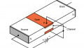
Biasing for n-channel FETs is shown at the right. Here we have our biasing. We have some voltages applied to this. Notice we have VDD this would be for the voltage on the drain. You'll notice there's a negative voltage connected to the n-material here and the positive on the other side of the N material. Current would flow through the N material as such. This would define the current in the drain. Another voltage is supplied and this voltage is between the gate and the channel. Notice that we have a positive here going to the N material and a negative going to the P. Now, this is a reverse bias configuration. This is reverse bias here. Notice we're showing one volt here. We're going to show increasing values of voltage here on screens that will follow after here.
The two parallel PN junctions are reverse bias causing a depletion region to form in the channel. Note positive on N and negative on P. We pointed that already. Since they had a reverse bias between the P and the N, we're going to have a depletion region at the borders of the PN and the N material. Now, this is low voltage. It's at 1 volt and we do have a depletion but it isn't very large.
Increased reverse biasing causes the depletion region to expand, increasing the resistance. As we increase the values of the voltage here, we're going to increase the depletion regions. Hence, we're going to increase the resistance of the N-channel. In this case, the VGG value is 1 volt. It is common for this value to be zero for max current flow hence there would be no verse bias. If this was at zero volts you would have maximum current flowing from source to drain. This is just opposite the way that a bipolar transistor would work. If you had zero volts on the base of a bipolar transistor, you would have no current flow. With a FET zero volts on the equivalent gate would make for maximum flow of current.
As the value of reverse bias from VGG increases, note that the depletion region increases and begins to choke the flow of current through the N material. Now it was 1 volt in the previous screen, now it is 3 volts. You'll notice that the depletion region here is becoming larger. Electrons want to go from here over to here but they're literally being choked. We're experiencing increasing resistance in the channel and decreasing flow of current through it. The behavior of the N-channel is much like a resistor. With low reverse bias, it has very little resistance to current flow. With increases in reverse bias the resistance increases.
Now we're at 3 volts of reverse bias. When a high level of reverse voltage is placed across the P-channel the N-channel is--here is an interesting term, “pinched off.” Here we have 6 volts here. Now the depletion regions have gotten so large that they have completely pinched off all flow and current flow through this device will cease. This is equivalent to the cutoff in a bipolar transistor. Of note, the N-channel has no specific kind of doping that differentiates between the drain and the source. In a bipolar transistor, there was a differing doping on the emitter and the collector. In this case, there is no differing. In most sets the drain and the source are interchangeable. Bipolar requires forward biased PN junction for conduction. JFET requires zero volts and we had mentioned that before.
This is our beginning point with FETs and we looked at the biasing and just a little bit about the construction of these devices.