Facebook
 Google
 GitHub
 Linkedin
The Physical Operation of Light-Sensitive pn Junctions
In this article, we’ll delve into semiconductor physics to better understand the operation of photodiodes.
This article is the second part of a series on photodiodes, the devices that create electrical signals when met with ambient light, laser signals, or light focused by a camera lens. In the first article, we discussed the nature of light and pn junctions. Now, we'll review the physical operation of light-sensitive pn junctions.
In the next few parts of the series, we will address:
- Two modes of photodiode operation: photoconductive and photovoltaic
- Characteristics of various photodiode technologies/semiconductors
- The photodiode equivalent circuit
The Silicon pn Junction
Interesting things happen when a piece of n-type silicon is in contact with a piece of p-type silicon: diffusion current flows from the p side to the n side, a depletion region forms, and drift current flows from the n side to the p side.
Diffusion Current
Holes are the majority carriers on the p side, and free electrons are the majority carriers on the n side. These carriers are subject to diffusion, i.e., the tendency for particles to move from higher concentration to lower concentration. Holes diffuse across the junction, from p to n, and electrons also diffuse across the junction, from n to p. These charge-carrier movements are a form of electric current; we call it diffusion current.
Diffusion current is described as flowing from the p side to the n side, because conventional current flows in the same direction as positive charge carriers, even if positive charge carriers are not actually present in the circuit.

In this case, holes are on the move, so we actually have positive charge carriers, and thus conventional current is more scientifically coherent than it is in circuits that do not contain diodes or transistors.
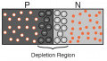
The Depletion Region
We have free electrons on the n side and holes on the p side. When free electrons diffuse across the junction, they meet up with holes on the other side. Electrons “fall” into holes, so to speak, and recombination occurs near the junction.
This leads to a region of overall negative charge near the junction on the p side, because recombination has eliminated holes that were previously balancing bound negative charges in the p-type semiconductor. The same thing happens on the other side, in the n-type semiconductor, except that over there, the bound charges are positive.

We call this the depletion region because the sections of overall positive and negative charge, on either side of the junction, result from the depletion of majority charge carriers, which in turn is the result of diffusion current and recombination.
Drift Current
Doping is not the only source of mobile charge carriers in a semiconductor. Thermal energy causes random generation of electron-hole pairs, leading to the presence of minority carriers, i.e., electrons on the p side and holes on the n side.
If a hole on the n side, or a free electron on the p side, makes its way into the depletion region, the depletion region’s electric field will reinforce motion toward the other side of the junction. This is drift current: minority carriers moving across the junction under the influence of an electric field. It flows from n side to p side.

So does current continuously flow through a diode, even when it’s totally unconnected from power sources and other components? Certainly not. A pn junction naturally maintains equilibrium between diffusion current and drift current. They flow in opposite directions with the same magnitude, so the net current is zero.
Light-Sensitive pn Junctions
When a junction is exposed to light, we have an additional source of mobile charge carriers, namely, the energy delivered by incoming photons. If a photon generates an electron-hole pair within or near the depletion region, the depletion region’s electric field can push the mobile charge carriers across the junction.
This is what we call photocurrent: current resulting from the movement of light-induced charge carriers.

Photocurrent is reverse current. Like drift current, it flows from n side to p side, and notice how it crosses the junction under the influence of the depletion region’s electric field, just as drift current does. We’ll return to drift current later in this introduction when we discuss dark current.
The Depletion Region in Photodiodes
As indicated above, light-generated electron-hole pairs contribute to photocurrent only if they are in or near the depletion region. This suggests that we can make a photodiode more sensitive by increasing the width of the depletion region: with a wider depletion region, the same intensity of incident light will generate more photocurrent, since more of the light-generated charge carriers are within reach of the electric field that pushes them across the junction.
There is another way in which the depletion region influences photodiode operation. A depletion region functions like a capacitor within a diode, and in a photodiode, this capacitance limits the device’s ability to respond to rapid variations in illuminance.
Thus, the depletion region is associated with two important considerations in the design of photodiode-based systems. I revisit these topics in the next article.
Recap
Diffusion current in a pn junction flows in the forward direction, and it produces a depletion region. The electric field in this depletion region allows for an equalizing current, called drift current, that flows in the reverse direction. Basic knowledge of drift current and the depletion region helps us to understand important aspects of photodiode implementation.
In the next article, we'll take a look at photovoltaic and photoconductive modes of photodiode operation.
Related Content