 Facebook
 Google
 GitHub
 Linkedin
JFET Amplifiers
Video Lectures created by Tim Feiegenbaum at North Seattle Community College.
Continuing our discussion of JFET with a look at three of the common configurations used in JFET Amplifiers. The JFET equivalents of bipolar transistor amplifier configurations are: Common-source and this would compare to the common-emitter in bipolar, the common-gate that would compare to the common-base, and then the common-drain which would compare to the common-collector in the bipolar.
First, we're going to look at the common-source amplifier. Again, this compares to the common-emitter amp. We'll note the CS bypass cap grounds the source for AC, hence the common-source. Remember the reason we called the common-emitter amp, the reason we gave it that name was because there was a capacitor tied directly to the emitter that went to ground. This was a ground for purposes of AC. Instead of common-emitter, we're calling it common-source. That is why.
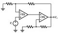
We have C1 and C0 that operate as coupling capacitors. C1 here couples the signal source to the gate and C0 couples the output to the load. You'll notice the load here, there's a reference of zero volts right here. At this point, it might be of note that--and we talked about this in common-emitter, that the drain is at a DC level. Let's pretend we have 10 volts positive here to make for maximum signal flow with these designs. These would probably be about five volts.
The output that's developed here, the AC, is going to be AC but it is going to be at a 5-volt level. If you were to look at an oscilloscope you would see 5 volts here, but at that 5-volt level, you would see this AC signal riding there. The reason that you have this output capacitor here, this coupling capacitor here is that you do not want that DC on the load. Remember that a capacitor does not pass DC only AC. The AC signal is passed across the cap and it goes to the load. Notice the reference here at zero volts.
The phase inversion is 180 degrees from input and output. This is no surprise. This is what we have with the common-emitter amplifier as well. This provides high voltage and power gain and it tends to be a little bit unstable in terms of current gain. Oftentimes they will place a component, another resistor in here that tends to swamp out those variations and current gain. That's also done with the common-emitter amp.
We continue here. Look, this is still the common-source amp. A few things that we need to mention: The gate of the JFET returns to ground through RG. Remember, we have the signal source here. Notice the RINT here. That represents the internal impedance of the signal source. Remember we talked about output impedance and how that when you generate a signal, part of that signal is actually dropped across the source. In this case, 500 ohms is how much of that signal will be dropped across a source. Notice the path. It goes from here through C1. Then there's a large 1 megohm resistor right here.
There are a couple of ways that that AC signal can go. It can go here. It can also go here. Recall that the gate-source junction does not pass current. It is an electrostatic difference that establishes the biasing for the drain and it established this depletion layer. The current flow is going to be through this lag right here. Recall, notice the large 1 megohm resistance right here and the small output impedance of the signal source. Most of that signal will be felt right here and delivered directly to the gate.
As current flows through RS and places a positive voltage on the gate. This reverse biases the GS junction required for operation. We're talking about this point right here. Recall that current is going to flow from the ground to the drain. In that process, current will be dropped across RS and RD. This will cause a voltage drop here. We'll just pretend this is a positive 10 volts. This will be a positive voltage right here. The gate has no DC biasing so it will be zero volts. In respect from gate to source, this positive voltage will act as the negative biasing required for the gate-source junction.
The gate has no loading effect since RG provides the ground. We talked about that already. As the input varies, the output changes across RD. We have an input that is varying our output will vary across the drain just like we did with a common-emitter amplifier.
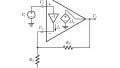
The common-gate, your text doesn't say much about this. It just shows it as an amplifier that parallels what we look at. In the common-base amplifier, remember, we have the base grounded and we injected a signal into the emitter. This is the same kind of configuration only we're injecting a signal into the source. We're having the gate grounded rather than the base.
Our final amp we're going to look at is the common-drain. Notice for purposes of AC going up to VDD, it's connected, and that looks like ground for purposes of AC. This is also referred to as the source follower. Recall that we looked at the emitter follower in bipolar. We have our signal source coming in. It goes to the gate. Then it goes to the source. Again, in this configuration, much like the emitter follower, there was no gain here. The thing that we got from this circuit was that it dropped the output down very low so that we could couple most of our signal. Here we have a load right here. This provides for excellent coupling so that most of the signal is not lost on the amp but is delivered directly to the load. This type of amp is very popular with high power amplifiers.
Summary of JFET Characteristics:
The source and drain terminals connect to the ends of the channel material in a JFET. Recall that the source and the drain in most JFETs are interchangeable. The gate-source junctions are reverse bias in a JFET. Increased reverse bias in a JFET causes the channel resistance to increase. The more reverse bias the more resistance it will have in the JFET channel. A JFET has maximum source-drain current with no bias, so with zero volts across the JFET you have maximum current. This is directly the opposite of what you see in common-emitter.
A JFET can be used in digital circuits by using saturation or cutoff modes. Common-source, gate, and drain configurations are comparable to bipolar amplifier configurations. Common-source amps have 180-degree phase inversion. Common-source amps have very high input impedance. Normal operation is such that current flows from source to drain. This concludes Section 10-2.
Related Content


Thanks, liked the clear the comparisons to bipolar. When you dropped in the 10V on the plus rail would have been nice to have added a 0 OR -10 on the “earth” side for absolute clarity. Appreciate the talk.