Facebook
 Google
 GitHub
 Linkedin
Exclusive Interview: Weebit Nano, TI, and the Future of Resistive RAM
Look out, flash! With a resounding vote of confidence from Texas Instruments and Onsemi, ReRAM may be here to stay.
Weebit Nano entered CES 2026 riding the high of a new licensing agreement with Texas Instruments. According to the company, the deal validates both the company’s products and the ReRAM industry as a whole, indicating a growing consensus that flash memory has reached its practical limits in power, scaling, and temperature tolerance.
At CES 2026, we spoke with Coby Hanoch, CEO of Weebit Nano, to learn about the TI agreement, the technical maturity of ReRAM, and how the company sees adoption accelerating over the next several years.
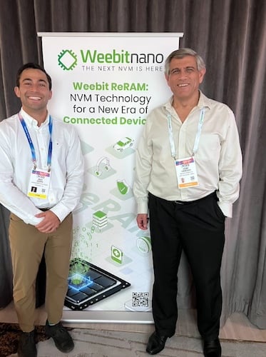
All About Circuits contributor Jake Hertz (left) with Weebit Nano CEO Coby Hanoch (right) at CES 2026.
A Licensing Milestone With Texas Instruments
According to the agreement, Weebit will license its embedded ReRAM IP to Texas Instruments for use in selected embedded processing products and process nodes. The scope includes technology transfer, design enablement, and qualification. While the deal itself is important for Weebit from a purely financial perspective, Hanoch says the significance goes much further.
“The biggest thing about the deal is not just TI, which is already a big, amazing thing,” Hanoch said. “It’s that now, the market is clear. ReRAM is the replacement for flash.”
Weebit’s ReRAM targets applications where embedded flash struggles, particularly at nodes below 28 nm and in environments that demand long retention at high temperature. The company has qualified its memory for AEC-Q100 operation at 150°C and has demonstrated retention up to 10 years under those conditions. Hanoch emphasized that TI’s involvement lowers perceived risk for the rest of the market.
“Customers always told us they wanted the technology, but someone else needed to be first,” he said. “Now someone else is first. After TI and Onsemi, it’s not such a big risk anymore.”
ReRAM Architecture and Performance Fundamentals
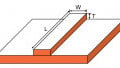
Weebit’s technology uses ReRAM as a back-end-of-line memory module, enabling integration without modifying the front-end transistor structures. That architectural choice reduces process disruption and keeps the added wafer cost to roughly 5%, compared with 20% or more for embedded flash. The ReRAM cell itself relies on a simple resistive-switching stack rather than a floating-gate architecture, enabling bit-addressable writes and eliminating block erase requirements.
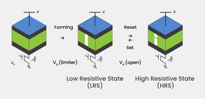
The working mechanism of a Weebit ReRAM cell. Image used courtesy of Weebit Nano
From a performance standpoint, Weebit reports write speeds up to 100x faster than embedded flash and an endurance of 100,000 to 1 million cycles. Power consumption drops sharply because the memory operates at low voltage with direct read and write access.
“Power, speed, endurance, temperature, and cost: on every axis that matters for embedded memory, ReRAM looks better than flash,” Hanoch said.
The company has also emphasized electromagnetic immunity as a differentiator relative to MRAM.
“We’ve seen cases where magnetic fields corrupted MRAM in consumer environments,” Hanoch said. “The biggest consumer companies made it very clear they were not willing to take that risk.”
Validation Through Foundries and IDMs
Before TI, Weebit licensed its technology to SkyWater and DB HiTek, then announced a partnership with Onsemi. Hanoch described that progression as deliberate.
“We went up an order of magnitude each time,” he said. “From SkyWater to DB HiTek to Onsemi and now to TI. Now we’re in the major league.”
Weebit completed a full technology transfer, tape-out, and working silicon at Onsemi's production fab in roughly nine months.
“That’s about as fast as it can be done,” Hanoch said. “They already have wafers and dies that work, with very good results.”
He attributed that speed to both demand and process compatibility.
“We said from day one we would use standard materials, standard tools, standard flows,” he said. “We didn’t want to give fabs excuses not to work with us.”
Embedded Memory for Advanced and AI Nodes
As process nodes shrink, embedded flash becomes less and less viable. To compensate, designers often pair the logic die with an external flash device, then copy data into SRAM at boot. Hanoch argued that ReRAM removes that architectural inefficiency.
“Replace the SRAM with ReRAM, and now you have a one-chip solution,” he said. “You boot instantly, you eliminate a security exposure, and you save power because the memory is non-volatile.”
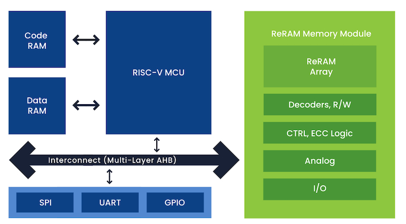
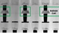
An embedded ReRAM demo chip. Image used courtesy of Weebit Nano
That change matters for edge AI devices built at 22 nm and below. ReRAM density exceeds that of SRAM, allowing more coefficients to reside on-chip.
“More bits on the same silicon means better accuracy for inference,” Hanoch said.
Additionally, the company has already demonstrated AI inference using its ReRAM in silicon and sees growing interest in near-memory and in-memory compute architectures.
“The ReRAM bit behaves like a synapse,” he said. “That makes it a natural fit for neuromorphic concepts.”
Market Adoption and Remaining Barriers
According to Weebit, industry analysts now project ReRAM revenue growth at a 45% CAGR over the next six years, eventually reaching nearly $1.7 billion. Weebit’s own revenue tracks with that trend, rising from about A$1 million in fiscal 2024 to A$4.4 million in fiscal 2025, with projections above A$10 million for fiscal 2026.
Despite the technical advantages, Hanoch acknowledged that adoption still faces inertia.
“The biggest barrier is human nature,” he said. “People know flash. They worry about a new company and a new technology.”
He argued that technical proof points already exist.
“We have silicon at 130 nm, 65 nm, and 22 nm. We’re qualified for mass production. Customers are designing products around our ReRAM today.”
Scaling the Organization for Parallel Customers
Over the past year, Weebit invested heavily in internal infrastructure to prepare for multiple simultaneous deployments. The company added formal project management, automated tracking, and a dedicated customer success organization led by former fab executives.
“This was the year we moved from spreadsheets to real systems,” Hanoch said. “Now we’re ready to sign many customers in parallel.”
Reflecting, Hanoch framed the TI agreement as validation and an inflection point.
“When TI and Onsemi commit, the perceived risk drops,” he said. “That’s why we expect 2026 and 2027 to be the years when ReRAM really moves into the mainstream.”