Facebook
 Google
 GitHub
 Linkedin
The Effect of MOS Non-Idealities on VLSI Circuit Reliability
Learn about various non-idealities of MOS transistors and the effects they have on VLSI system reliability.
Reliability is the guarantee that a system will continue operating correctly for a certain amount of time. In this article, we are going to discuss MOS (metal-oxide-semiconductor) non-idealities as a failure mechanism in VLSI (very-large-scale integration) systems and how they affect system reliability.
Oxide Wear Out
As discussed in the previous article on non-idealities in VLSI circuits, a gate oxide can be a few atoms thick in incredibly small transistors. While this enables device miniaturization, it also causes leakage due to current tunneling.
Additionally, as a device ages, this non-ideality becomes worse because the oxide wears out. As a result, the threshold voltage shifts, which further increases the gate leakage. A more significant impact of this effect is that transistor mismatch or high leakage current can cause circuit failure.
The three main causes of oxide wear out are:
- Hot carriers
- Negative-bias temperature instability (NBTI)
- Time-dependent dielectric breakdown (TDDB)
Hot Carriers
In fast VLSI circuits, transistors switch millions of times per second. During switching, high-energy carriers (electrons or holes), which are known as “hot carriers,” are easily injected and trapped in the gate oxide. This hot-carrier injection causes impurities in the gate oxide, thereby changing the I–V characteristics of the device.
This injection causes several problems. It makes the NMOS transistor operate more slowly, causing a mismatch in the circuit. It also causes a high-current surge in PMOS transistors, which can lead to critical circuit failure.
To simulate or model hot carriers in the VLSI circuit, an analytical approach has been proposed by Hsu et. al (1991 and 1992) and Quader et. al.
Negative-Bias Temperature Instability (NBTI)
NBTI causes an increase in threshold voltage, mobility degradation, drain current, and transconductance of p-channel MOS transistors. NGTI occurs in the presence of traps at the silicon/silicon oxide interface at high temperatures.
This effect is more prominent in PMOS transistors due to strong negative bias (gate voltage of 0 and source voltage of VDD) at elevated temperatures. The major effect of NBTI is that it leads to mobility reduction and increased threshold voltage, which results in increased delay in digital circuits.
According to Alam and Mahapatra; Jeppson and Svensson; and Ogawa and Shiono; NBTI can be modeled using the Reaction-Diffusion (R-D) model. Paul et. al also propose that the threshold voltage shift can be modeled as
$$\Delta V_t = ke^{\frac{E_{ox}}{E_0}}t^{0.25}$$
Time-Dependent Dielectric Breakdown (TDDB)
TDDB refers to the physical process whereby a dielectric stored under a constant electric field, which is less than the material breakdown strength, will break down with time.
In MOS transistors, the gate oxide is the dielectric; when an electric field is applied across the gate oxide, the current will gradually increase. When the electric field is applied for a certain amount of time, it can lead to a serious dielectric breakdown that short circuits the gate.
Two main models have been proposed for the electric field dependence of TDDB: the anode hole injection (AHI) model and the Eox model. A revised study for these models was conducted in Moonen et al.
Electromigration
Electromigration occurs often in wires carrying unidirectional current (DC). During operation, interconnects usually experience an “electron wind” because of high current densities that cause metal atoms to migrate over time. It is usually observable by checking for the formation of voids (Hu et. al).
Figure 1 shows a micrograph showing an electromigration failure of a via between M2 and M3 layers (Christiansen et. al).

Figure 1. Electromigration failure of M2-M3. Image used courtesy of Christiansen et. al
The presence of a void will increase the resistance of the interconnection, and the presence of a hillock will cause a short circuit between different levels of interconnection (Jaikaran et. al).
Since electromigration depends on current density, J. Black proposed a model for computing the maximum allowable current given by DC density Jdc for a given mean-time-to-failure (MTTF) and operating temperature T.
$$MTTF\propto\frac{e^{\frac{E_a}{kT}}}{J^n_{dc}}$$
Where Ea is activation energy
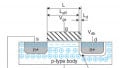
Latch-Up
Latch-up is a type of short-circuiting that occurs in CMOS chips. The tendency of CMOS to develop a low-resistance path between VDD and GND causes serious meltdown and increases the failure rate of an IC. Theoretically, latch-up occurs when parasitic bipolar transistors formed by the substrate, well, and diffusion turn ON.
Figure 2 shows the equivalent circuit of the BJT pair formed in a CMOS inverter.

Figure 2. Model of CMOS latch-up
In addition to the NMOS and PMOS transistors, the circuit consists of a PNP and an NPN transistor connected to two resistors, which are connected between power and ground rails. The resistors are due to the resistance between nearby substrates and well taps.
Ordinarily, the BJT transistors are OFF. But when current flows through the substrates (Rsub), Vsub will rise, which will turn ON the NPN transistor. As a result, the NPN transistor pulls current through Rwell, thereby turning ON the PNP transistor.
The PNP transistor will also pull current through Rsub, thereby raising Vsub. This cycle creates a positive feedback loop, causing a large current to flow back and forth between VDD and GND. If this cycle continues for a long time, it generates heat and melts down the power rails.
Fortunately, latch-up can be prevented by reducing the resistance between the substrate and the well. The common way to achieve this is to place the substrate and well taps close to each transistor (Neil and David).
In some applications, guard rings as shown in Figure 3 are suitable to surround the transistor and provide the low-resistance path between the transistor and the power rail.

Figure 3. Guard rings
Conclusion
So far, we have discussed non-idealities of MOS transistors and how they affect the reliability of VLSI systems. Several models have been discussed on how to measure and simulate their impact on designs.
Fortunately, modern SPICE models and CAD tools are thorough and accurate in predicting the performance of various designs into the gigahertz range while accounting for the effect of these non-idealities. Leveraging these tools may drive automation and faster design time in the chip development lifecycle.
References
- Alam, M. A., & Mahapatra, S. (2005). A comprehensive model of PMOS NBTI degradation. Microelectronics Reliability, 45, 71–81.
- B. Paul, Kunhyuk Kang, H. Kufluoglu, M. Alam, and K. Roy, “Negative bias temperature instability: estimation and design for improved reliability of nanoscale circuits,” IEEE Trans. CAD, vol. 26, no. 4, Apr. 2007, pp. 743–751.
- C. Christiansen, J. Gambino, J. Therrien, D. Hunt, and J. Gill, “Effect of wire thickness on electromigration and stress migration lifetime of Cu,” Proc. Failure Analysis of Integrated Circuits, Jul. 2006, pp. 349–354
- Hu, C., Rodbell, K., Sullivan, T., Lee, K., & Bouldin, D. (1995). Electromigration and stress-induced voiding in fine Al and Al-alloy thin-film lines. IBM J. Research and Development, 39 (4), 465–497.
- Jaikaran, S., Mukesh, T., & Madhu, S. (2012). Impact of MOSFET Non-Ideal Characteristic Breakdown on Digital Circuit Operation and Reliability. International Journal of Electronics Communication and Computer Engineering, 818–822.
- J. Black, “Electromigration—A brief survey and some recent results,” IEEE Trans. Electron Devices, vol. ED-16, no. 4, Apr. 1969, pp. 338–347.
- Jeppson, K. O., & Svensson, C. M. (1977). Negative bias stress of MOS devices at high electric fields and degradation of MNOS devices. Journal of Applied Physics, 48, 2004–2015.
- K. Quader, E. Minami, W. Huang, P. Ko, and C. Hu, “Hot-carrier-reliability design guidelines for CMOS logic circuits,” JSSC, vol. 29, no. 3, Mar. 1994, pp. 253–262.
- Moonen, R., Vanmeerbeek, P., Lekens, G., De Ceuninck, W., Moens, P., & Boutsen, J. (2007). Study of Time-Dependent Dielectric Breakdown on Gate Oxide Capacitors at High Temperature. 14th International Symposium on the Physical and Failure Analysis of Integrated Circuits, 288–291.
- Neil, W., & David, H. M. (2011). CMOS VLSI Design (4th ed.). Boston: Addison-Wesley.
- Ogawa, S., & Shiono, N. (1995). Generalized diffusion-reaction model for the low-field charge build-up instability at the Si–SiO2 interface. Physics Rev, 51, 4218–4230.
- Schroder, D. K. (2007). Negative bias temperature instability: What do we understand? Microelectronics Reliability, 47 (6), 841–852.
- W. Hsu, B. Sheu, & S. Gowda, and C. Hwang, “Advanced integrated-circuit reliability simulation including dynamic stress effects,” JSSC, vol. 27, no. 3, Mar. 1992, pp. 247–257.
- W. Hsu, B. Sheu, & S. Gowda, “Design of reliable VLSI circuits using simulation techniques,” JSSC, vol. 26, no. 3, Mar. 1991, pp. 452–457.
Related Content