Facebook
 Google
 GitHub
 Linkedin
Non-Idealities in VLSI Circuits
This article discusses VLSI (very-large-scale integration) circuits and the sources of non-idealities that affect MOS transistors.
Since the discovery of transistor in the late 1940s to early 1950s, it has been the most dominant component in electronic devices, and it has enabled a terrific improvement in modern-day technology. Moore’s law and Dennard scaling have described the need to improve the feature size and performance of the transistors found in modern-day IC design; that is, the need to double the number of transistors in a particular chip every 24 months.
Due to this improvement, there are obvious differences between the performance, operating point, and intrinsic properties of earlier transistor circuits (which were few millimeters) when compared to modern-day transistor circuits (which are only a few nanometers across).
In this article, we are going to discuss the ideal MOS transistor analysis model and the non-idealities that have arisen due to the constant improvement in feature size and design of MOS transistors. Also, we are going to discuss the sources of non-idealities (SNIs) in MOS transistors are introduced design methods to properly model VLSI circuit in simulation before actual implementation.
Background Information: Source and Drain
Consider the basic transistor diagram in Figure 1. When no voltage is applied to the gate (g), the transistor is said to be in the OFF state.
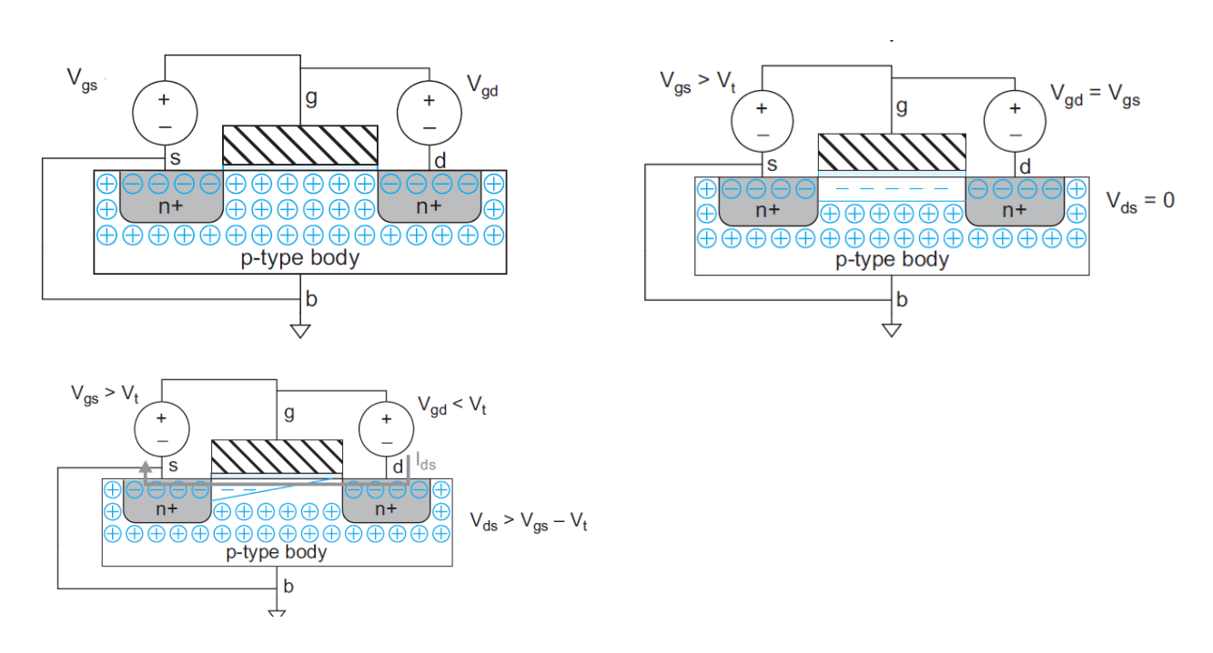
Figure 1. Basic transistor operating mode
If a small gate voltage (Vgs < Vt) is applied, this voltage level is called subthreshold voltage level and the transistor is still assumed to be OFF (no conduction). But if a voltage high enough to get its carrier (electron or holes) moving is applied (Vgs > Vt), it creates a channel between the drain (d) and the source (s), hence making the drain-source current (Ids) to flow. At this point, the transistor is said to be in the ON (active) state, for example. This is similar to whenever you turn ON your smartphone.
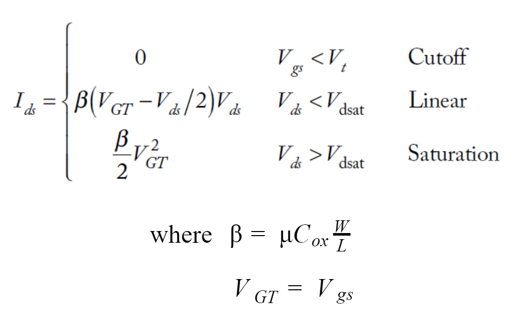
In the ON state, the drain current (Ids) increases linearly with the drain voltage (Vds) until (Vds = Vgs= Vdsat), after which the drain current remains constant. If the drain voltage is increased further to the value (Vds > Vdsat), at this point, the transistor will probably produce its maximum current limit, hence, the transistor is said to be in the saturation mode. For example, if you keep on consuming a lot of food, there is a maximum amount of work you can do based on your physical limitation, which means any more food you consume is assumed to be wasted. Similarly, the transistor is constrained by its physical limitation such as its feature size (W and L) and its doping level (the amount of impurities it contains).
Consequently, this illustration is termed as the long channel model and the drain-source current for a transistor whose gate is of length (L) and width (W) is given by
Motivation
IC designers try to vary the W/L of a transistor to fit in more components on a chip. The more they try to cram transistors onto a chip, the more they face the physical limitations of the transistors.
So, over the years, as transistor sizes move from micrometer to nanometer technology, the majority of the assumptions stated above do not perfectly mimic the operation of a real transistor. For example, when the transistor is said to be in the OFF state, the current is assumed to be zero but in the actual sense, there is subthreshold current leakage between the terminals of the transistor which are ideally negligible, in the order of nanoampere (nA) but when multiplied by the millions-billions of transistors in a device, they are significant.
For instance, you want to keep your battery at the level you left it when you turn off your smartphone, so, the leakage current is an issue designer must deal with when simulating their design. Secondly, a transistor is said to keep its maximum current constant in the saturation mode, but in real transistors, the current has been observed to increase at a slower rate which defeats the purpose of supplying a constant amount of current.
Therefore, in this section, we are going to each of the mechanisms responsible for these non-ideal behaviors and how designers can correctly model transistors for simulation in their design flow.
Velocity Saturation and Mobility Degradation
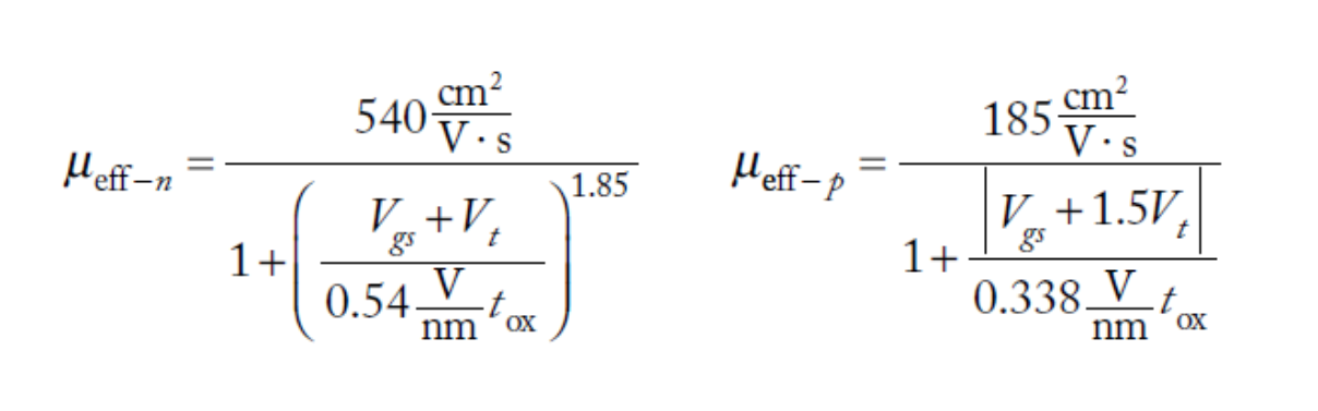
Velocity saturation results in lower Ids at high Vds (saturation mode). Because higher voltage causes higher electric field strength along the channel, which causes the carrier to collide more often, hence results in mobility degradation of the carrier.
The carrier is also having physical limitation hence it can only maintain a certain maximum average speed, this is called velocity saturation. A universal model that matches this scenario is given in (Chen, et al., 1997) and (Chen, Hu, Fang, Lin, & Wollesen, 1997), where the mobility (µ) was replaced by the effective mobility (µeff).
Channel Length Modulation
In an ideal transistor, Ids is independent of Vds when the transistor is in saturation mode, making the transistor a constant current source. But in reality, Vds (drain-source voltage) causes a depletion layer (Ld) along the walls of the channel, which makes the effective channel length less than the actual channel length, thereby making the effective length (Leff = L – Ld).
Consequently, as Vds increases, Leff gets relatively shorter, hence causing reduced lateral field strength. Since electric field strength (E) is proportional to the length of the channel. This reduced field strength pushes Ids variability back to the linear region, which makes Ids increases with Vds in saturation.
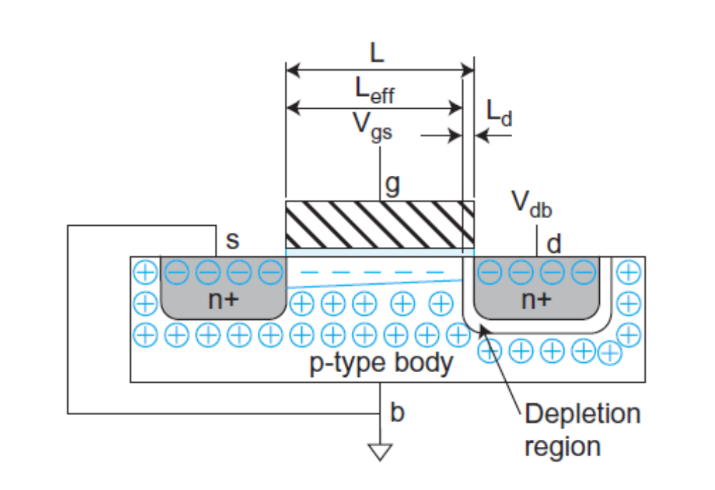
Figure 2. Depletion region shortening effective channel length
In this case, Ids can be better modeled by multiplying it by a factor dependent in the early voltage VA as described in (Gray, Hurst, Lewis, & Meyer, 2001).
Threshold Voltage (Vt) Effect
Ideally, the threshold voltage (Vt) has been treated to be constant but actually, it varies with the body voltage (source-body voltage, Vsb), drain voltage, and even the channel length.
Firstly, from the transistor in Figure 2 above, when Vsb is applied, it increases the threshold voltage (Vt) required for the transistor to turn ON. With this in mind, Vt can be re-modeled as
$$V_t = V_{t0} + \gamma (\sqrt[2]{Ø_0 + V_{sb}} - \sqrt Ø_s)$$
More information can be found in (Tsividis, 1999).
Secondly, the drain voltage which created an electric field along the channel causes what is known as Drain-Induced Barrier Lowering (DIBL) which causes the threshold voltage to reduce by a factor represented as DIBL coefficient.
$$V_t = V_{t0} - \eta V_{ds}$$
$$\eta$$ = DIBL coefficient
Typically, Vt increases with the channel length, but as Vds is applied, channel length decreases due to the presence of the depletion region and hence, causes what is called Vsb roll-off (reduction).
Leakage
When the transistor is OFF, it is assumed that the drain-source current is zero. In the actual sense, they leak a small amount of current due to subthreshold conduction and junction leakage.
For subthreshold leakage, it is assumed that the current Ids are zero when Vgs < Vt, but in reality, the current drops faster in this operating condition. As Vgs lowers to a negative value, it forms what is called weak inversion as shown in Figure 3:
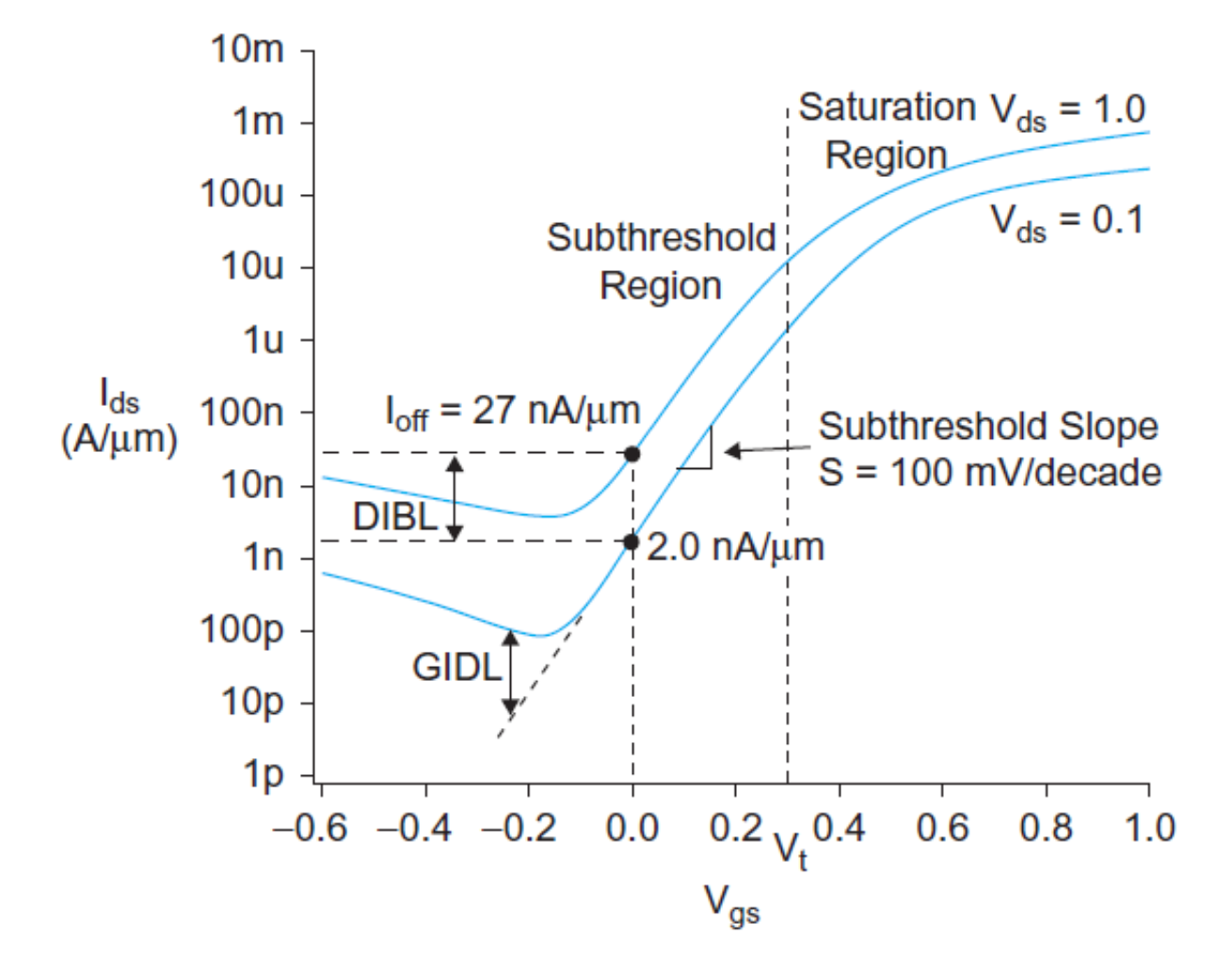
Figure 3. IV-characteristic showing exponential fall of Ids at Vgs < Vt
For junction leakage, we observed that the transistor is a basic PN/NP junction diode between the diffusion and substrate/well. When the transistor is in the OFF state, the source-gate junction diode is reverse biased. However, reverse-biased diodes still conduct a small amount of current given from the classical diode equation:
$$I_D = I_S (e^\frac{V_D}{V_T} - 1)$$
Temperature is also a huge mechanism of non-idealities as it majorly affects other non-idealities discussed so far. For example, subthreshold leakage increases with temperature. The threshold voltage (Vt) also decreases with temperature which makes it susceptible to DIBL and subthreshold conduction. Generally, it is more suitable to operate at a low temperature as it significantly reduces velocity saturation and mobility degradation.
Geometry Dependence
The layout designer usually draws a transistor with a certain channel length (Ldrawn) and width (Wdrawn). But the actual gate/channel length dimension might defer based on the manufacturing process. This would cause the transistor to have less/more of the intended dimension, hence it will affect the threshold voltage and effective channel length and velocity saturation effect which could cause some non-idealities as discussed in previous sections. This non-ideality is modeled as shown below; LD and WD are dependent on the manufacturing process.
$$L_{eff} = L_{drawn} + X_L - 2L_D$$
$$W_{eff}= W_{drawn} + X_W - 2W_D$$
References
- Chen, K., Hu, C., Fang, P., Lin, M., & Wollesen, D. (1997). Predicting CMOS speed with gate oxide and voltage scaling and interconnect loading effects. IEEE Trans. Electron Devices, 44(11), 1951-1957.
- Chen, K., Wann, H., Dunster, J., Ko, P., Hu, C., & Yoshida, M. (1997). MOSFET carrier mobility model based on gate oxide thickness, threshold and gate voltages. Solid-State Electronics, 39(10), 1515-1518.
- Gray, P., Hurst, P., Lewis, S., & Meyer, R. (2001). Analysis and Design of Analog Integrated Circuits (4th ed.). New York: John Wiley & Sons.
- Neil, W., & David , H. M. (2011). CMOS VLSI Design (4th ed.). Boston: Addison-Wesley.
- Tsividis, Y. (1999). Operation and Modeling of the MOS Transistor (2nd ed.). Boston: McGraw-Hill.
Related Content