Facebook
 Google
 GitHub
 Linkedin
Simulating Pulse-Frequency Modulation for DC-DC Converters
Using a pulse-frequency-modulated buck converter as an example, this article describes techniques for incorporating PFM into switching regulator design and simulations.
My preceding article explained the characteristics and objectives of pulse-frequency modulation. In this article, I’ll bring LTspice into the discussion. We’ll examine some useful schematics for working with PFM, then run simulations and analyze the results.
A PFM Buck Converter
If you’ve read my guide to simulating a buck converter, Figure 1 may look familiar—the PWM buck converter we examined in that article has the same general structure as the circuit below.
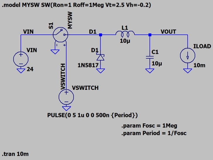
Figure 1. A PFM buck converter implemented in LTspice.
Because we’re using PFM, though, I have different parameters for the Pulse function. This is a fixed-on-time PFM scheme with on-time at 500 ns, and the starting period is 1 μs.
The initial settings are identical to PWM control with a switch frequency of 1 MHz (period of 1 μs) and 50% duty cycle. As previously stated, though, we’re not using PWM—so when we start making adjustments, we won’t modify the duty cycle while keeping pulse frequency constant. Instead, we’ll modify the frequency. This will result in duty cycle changing as well, since:
$$\text{Duty Cycle}~=~\frac{\text{On-Time}}{\text{Period}}$$
and the period is inversely proportional to the frequency. In this example, because the period will increase while the on-time stays fixed at 500 ns, the duty cycle will decrease.
Figure 2 shows the VOUT behavior of our PFM buck converter.
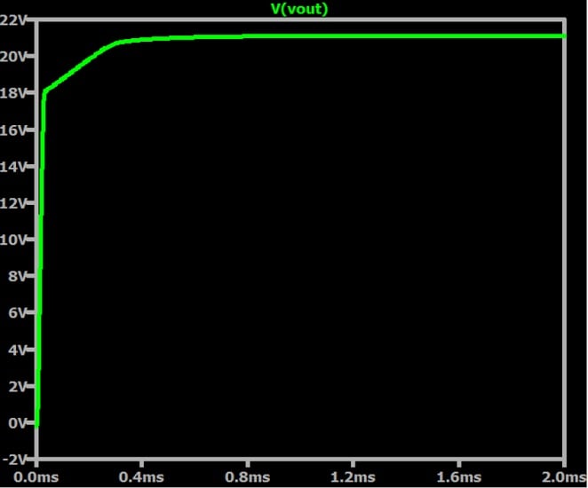
Figure 2. Output voltage for a pulse-frequency-modulated buck converter.
With only 10 mA of load current, the 50% duty cycle switch-control waveform produces an output voltage not much lower than the input voltage. To produce an output voltage value more consistent with the theoretical relationship between duty cycle and VIN-to-VOUT ratio, we would need to significantly increase the load current.
Figure 3 shows the output ripple and how it aligns with the switching action.
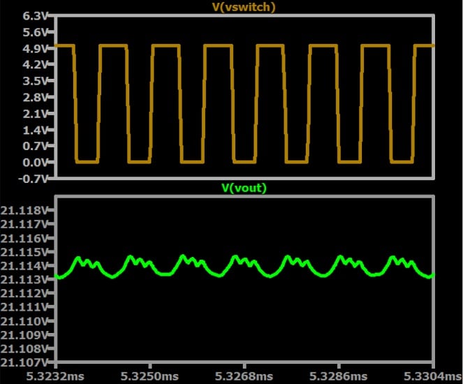
Figure 3. Switching voltage (top) and output voltage (bottom) for a PFM buck converter.
Decreasing the Pulse Frequency
PFM is beneficial during low-load-current situations because the reduced switching frequency translates to fewer transitions and therefore lower switching losses. The overall result is higher efficiency than could be achieved with PWM, which has the same number of transitions regardless of load current.
Figure 4 shows what happens to VOUT if I change the FOSC parameter from 1 MHz to 100 kHz.
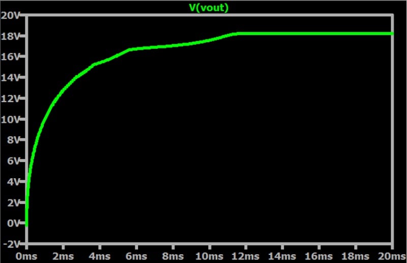
Figure 4. PFM buck converter output voltage with FOSC = 100 kHz.
The output voltage has dropped a bit, but overall the circuit still works quite well even though we decreased the frequency of pulses by an order of magnitude. Meanwhile, the lower switching frequency greatly reduces the amount of energy wasted by switch transitions.
To help demonstrate how PFM operates in a switching regulator, I’ll further reduce the switching frequency to 10 kHz and increase the load current from 10 to 100 mA. These are drastic changes—you can see the results in Figure 5.
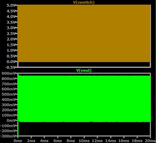
Figure 5. PFM buck converter switching and output voltage. FOSC = 10 kHz, ILOAD = 100 mA.
Things aren’t looking too good anymore. Let’s zoom in and see what happened (Figure 6).
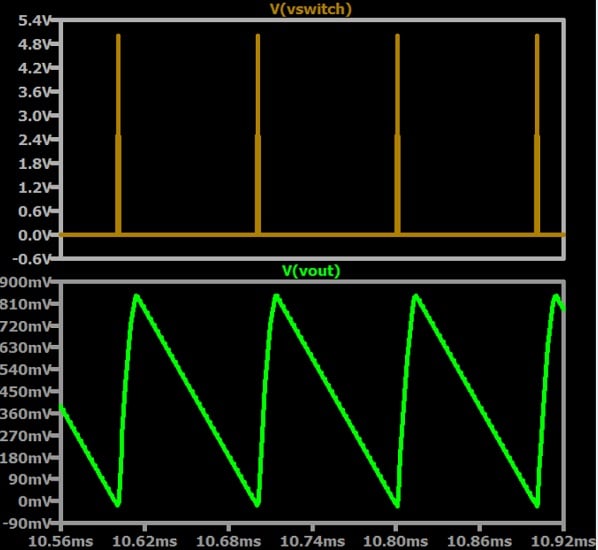
Figure 6. Magnified view of the switching voltage and output voltage from Figure 5.
I find this plot particularly illustrative. Each switching pulse draws energy from the input supply and transfers it to the output portion of the circuit, which needs this energy to supply the load current. However, because the pulse’s active duration is so short relative to its inactive duration, the energy is drained during each cycle. Consequently, the converter can’t maintain a stable output voltage.
If we leave the load current at 100 mA and increase the FOSC parameter back to 100 kHz, we see the same basic behavior. Now, though, the converter is able to produce about 6 V of steady output voltage with tolerable ripple magnitude (Figure 7).
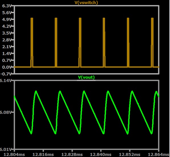
Figure 7. PFM buck converter switching and output voltage. FOSC = 100 kHz, ILOAD = 100 mA.
These plots help convey the fundamental operational dynamics of PFM voltage conversion. Each pulse transfers energy, in the form of electric current, to the output side. Reducing the frequency of these pulses improves efficiency, but the pulses must still occur frequently enough to keep up with the energy requirements of the load circuitry.
A One-Shot Circuit for PFM Control
The plots of VSWITCH with very low pulse frequency help us to recognize that PFM, unlike PWM, doesn’t require a continuously operating oscillator, and that a PFM control waveform isn’t really a typical oscillator signal. Instead, it’s more like a sequence of widely separated one-shot pulses. If these pulses are triggered by output conditions rather than a clock signal, we can improve efficiency further by reducing the quiescent current consumed by the regulator’s control circuitry.
A pulse generator can come in handy if you want to integrate some closed-loop functionality into PFM-based regulator simulations. Figure 8 illustrates a method for creating a triggered pulse generator in LTspice.
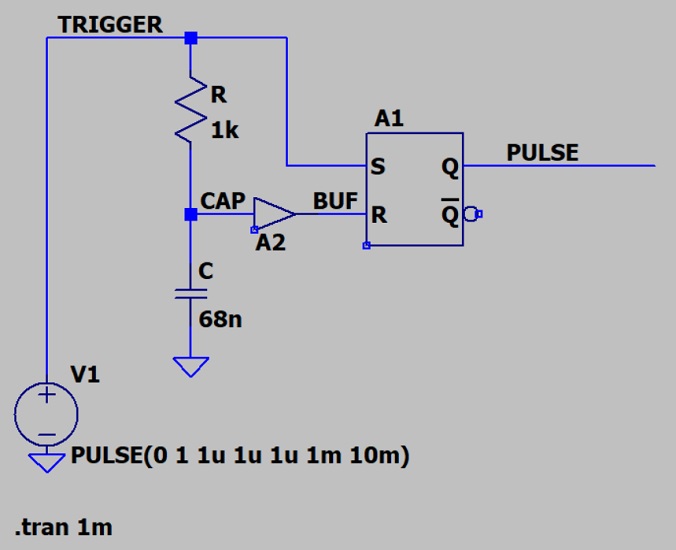
Figure 8. A triggered pulse generator implemented in LTspice.
Figure 9 demonstrates the circuit’s mode of operation. When the trigger signal (VTRIGGER) goes high, so does the output of the SR latch (VPULSE). The trigger signal also charges the capacitor (VCAP) through the resistor. When the voltage across the capacitor reaches 0.5 V (LTspice’s default logic threshold), the buffer output (VBUF) becomes logic-high and resets the latch, driving VPULSE back to a logic-low state.
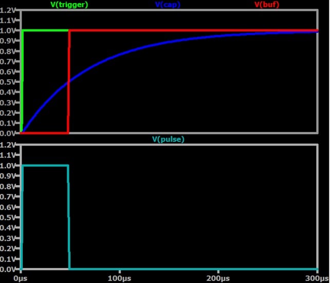
Figure 9. Triggered pulse generator operation.
You can control the width of the output pulse by changing the value of the resistor or capacitor. Note that the trigger signal’s logic-high duration must be longer than the pulse width.
Wrapping Up
Pulse-frequency modulation is an important technique for high-efficiency switch-mode regulators. We’ve looked at SPICE implementations of a PFM-controlled buck converter and a simple pulse generator; if you pursue this topic with additional simulations, I encourage you to leave a comment below and share your findings.
All images used courtesy of Robert Keim