 Facebook
 Google
 GitHub
 Linkedin
Using LTSpice for Amplifier Noise Measurement
Learn how to measure noise using LTspice for op-amp circuits with handy examples.
Learn how to measure noise using LTspice for op-amp circuits with handy examples.
In previous articles, we introduced modeling noise with LTspice and simulating noise sources in LTspice. This article shows how to use LTspice to measure the noise of an op-amp and of an op-amp combined with a dual-JFET input stage. How accurate are the measurements? Are they useful? To find out, the results are compared to noise specifications in datasheets.
An excellent summary of op-amp noise and how noise sources combine can be found in this article and app note from Analog Devices. An excellent explanation of converting an RMS value to peak-to-peak is in this video from Analog Devices.
LTspice Noise Simulation Example: Low-Noise Op-Amp
The first component to test is a low-noise op-amp. The circuit is a standard non-inverting amplifier with a resistance in series with the non-inverting input to measure bias current noise.
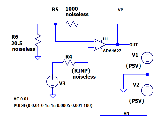
The values for the power supplies and input resistor have been parameterized to make them easy to change and use in .STEP directives. More on this later. Why is “noiseless” added to the resistor values? Adding this undocumented attribute to a resistor tells LTspice to ignore the resistor as a noise source. This feature is very useful because the extra noise from resistors does not have to be subtracted from the measurement. The noiseless attribute can be added using the Component Attribute Editor. Start this editor by holding down the control key and right-clicking on the resistor body. Add the word “noiseless” as an additional value. With this feature, the ONLY noise source is the op-amp. Perfect!
The op-amp is an Analog Devices ADA4627. Not a lot of work went into choosing this part. The ADA4627 caught my attention from a quick scan of the low-noise op-amp selection table from Analog Devices. It has low noise and supports supply voltages from ±5V to ±15V. Then, a check of the datasheet showed the noise is well specified. It was not chosen because the datasheet specs did or did not match LTspice testing.
Here is the noise section of the ADA4627 datasheet. The left column is for “B Grade” parts and the right is for “A Grade” parts. The specifications are used in the comparison table below.
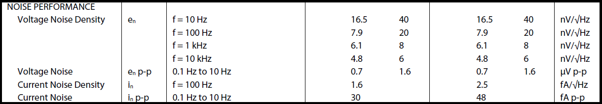
The table is from the Analog Devices ADA4627 datasheet
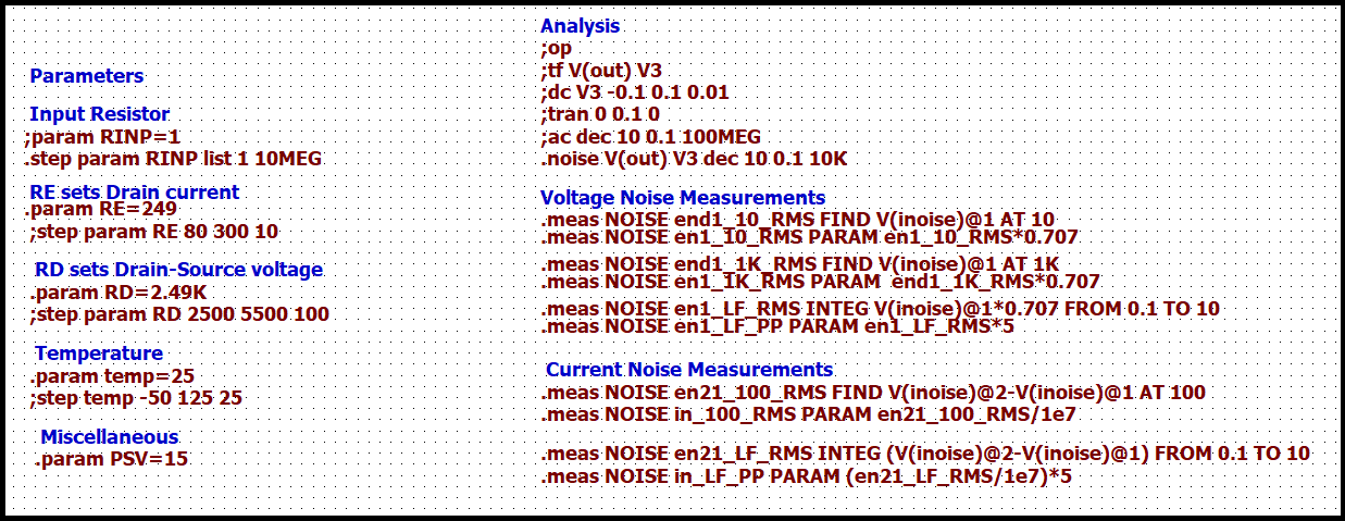
Here are the LTspice directives used in the simulation.
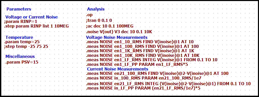
Measurement conditions are set with statements on the left-hand side. .PARAM statements provide values to the variables in the schematic. These are the variable names in curly braces, for example, {RINP}. .STEP statements run multiple simulations with different variable values. For example, two runs are done with different values of the input resistor. There is a small value for the input voltage noise measurement (Step #1) and a large value for the input current noise measurement (Step #2).
Measurements are specified with .MEAS statements on the right-hand side. No additional calculations are required to compare with the datasheet. I won’t go into the details of each .MEAS statement. However, let’s look at one to get the input voltage noise at 1kHz.
.meas NOISE en1_1k_RMS FIND V(inoise)@1 AT 1K
NOISE - Apply the measurement to a noise simulation
en1_1k_RMS - Just a name for the result. Used in the log file.
FIND - Specifies the measurement, which in this case is just getting a data value
V(inoise)@1 - The data set to use in the measurement. Details are below.
AT 1K - Selects the frequency of the data
Now for the magic. Click on the running engineer.
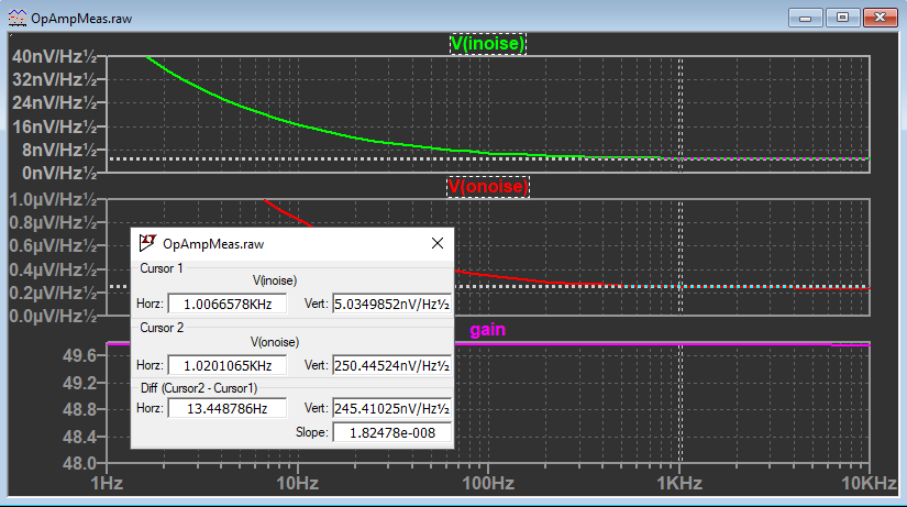
Here is a plot showing results from the two-step simulation. The green trace is Step #1 with a 1Ω input resistor. The purple trace is Step #2 with a 10MΩ input resistor. The red trace shows the difference between the two runs.
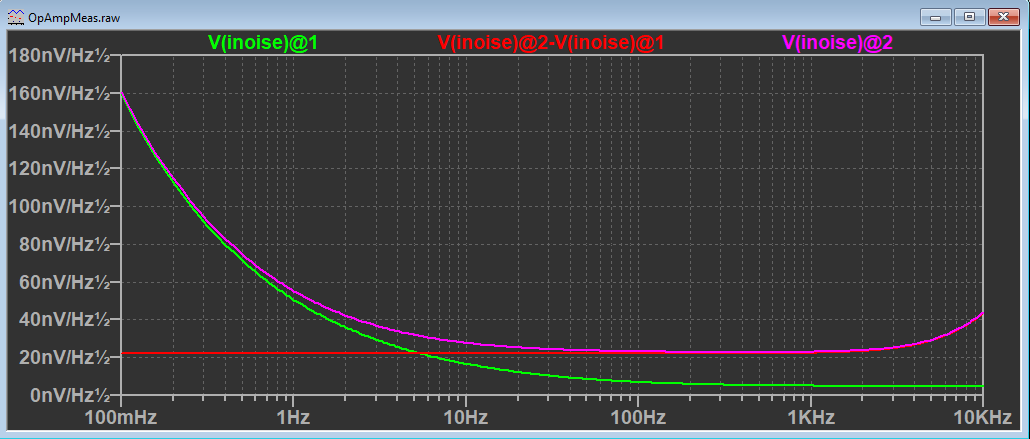
“V(inoise)” needs an explanation. “V(inoise)” is the output voltage noise of the entire circuit referred back to the input. This is calculated by LTspice for every noise simulation. This is explained further below. Remember the noise sources add and subtract in an RMS fashion. As one noise source gets larger than another, it starts to completely dominate. No problem! LTspice takes care of the calculation for us!
The data for a particular .STEP run is selected by adding “@1” or “@2” after a source. For example, “@1” is the run with the small input resistor.
The data from the .MEAS statements are found in the Spice Error Log. Here is a table comparing the datasheet values to the measured values. Not bad!
| Specification | Datasheet Value B Grade (Typ) | LTspice Measurement |
|---|---|---|
| Voltage Noise Density 10 Hz | 16.5 nV/√Hz | 16.6 nV/√Hz |
| Voltage Noise Density 100 Hz | 7.9 nV/√Hz | 6.9 nV/√Hz |
| Voltage Noise Density 1 kHz | 6.1 nV/√Hz | 5.0 nV/√Hz |
| Voltage Noise Density 10 kHz | 4.8 nV/√Hz | 4.8 nV/√Hz |
| Voltage Noise 0.1 to 10 Hz | 0.7 μV p-p | 0.55 μV p-p |
| Current Noise Density 100 Hz | 1.6 fA/√Hz | 2.2 fA/√Hz |
| Current Noise 0.1 to 10 Hz | 30 fA p-p | 35 fA p-p |
The datasheet gives peak-to-peak values for noise from 0.1 to 10 Hz (1/ƒ region) but LTspice calculates RMS. I applied a factor of 5 to convert RMS to peak-to-peak. The voltage noise is the same for the A and B grades. However, the current noise is different. The B grade is shown in the table.
The measurement results are in the “Spice Error Log”. Open this file by selecting the plot window and select View->Spice Error Log. Scroll down to the .MEAS results. Here is the entry for the voltage noise measurement explained above.
Directive on the schematic:
.meas NOISE en1_1K_RMS FIND V(inoise)@1 AT 1K
Corresponding Spice Error Log entry:
Measurement: en1_1k_RMS
             step v(inoise)@1    at
             5.03632e-009    1000
             5.03632e-009    1000
Measurement results are shown for each step. However, in these runs, the Step #2 value is overridden with the Step #1 value since the data is specified with the “@1” specification.
What is the “V(inoise)” source in the .MEAS directives? From the LTspice Help, V(inoise) is a calculation of “input-referred noise voltage density”. This noise source is the output noise referred back to the input for ALL noise sources in the circuit. However, since all the resistors are “noiseless”, the noise is only the input noise of the op-amp. Again, perfect!
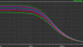
Here are plots to explain “V(inoise)” or “Input-referred noise voltage density”. V(inoise), V(onoise), and gain are shown in separate windows. Measurement cursors for V(inoise) and V(onoise) are placed at 1kHz. Dividing the output noise V(onoise) by V(inoise) is the circuit gain of 50. V(inoise) is the input noise from the op-amp since all the resistors are “noiseless”.
LTspice Noise Simulation Example 2: Low-Noise JFET Op-Amp
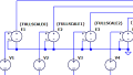
The next component to test is a very-low-noise dual JFET. Here is a diagram of the circuit.
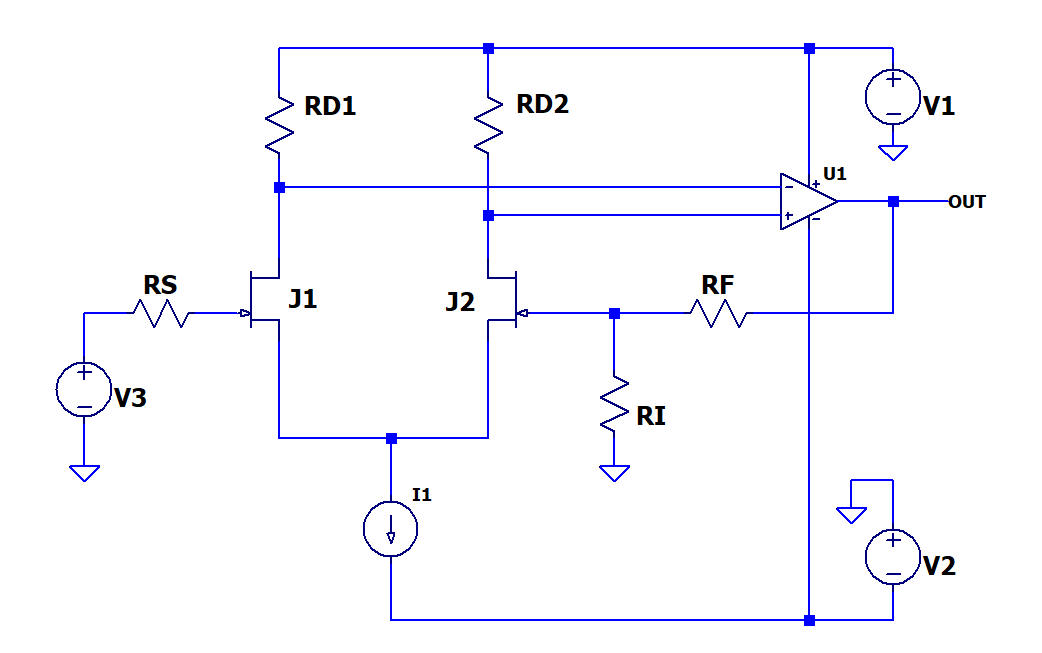
Here are key points that make the noise measurement almost the same as that of the op-amp circuit.
- The gain of the differential pair is large enough that the noise of the op-amp is very small compared to the amplified JFET noise and can be ignored.
- The noise of the current source biasing the JFETs (I1) is common to both of the op-amp inputs and is eliminated by the common-mode rejection of the op-amp.
- Noise from the drain resistors (RD1, RD2) is eliminated with the LTspice “noiseless” attribute.
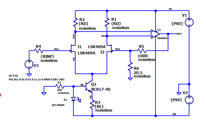
The dual JFET is the LSK489 from Linear Integrated Systems. This part was chosen because it is in the standard LTspice library and is a very-low-noise device. It was not chosen because the datasheet specs did or did not match LTspice testing. Here is the full schematic.
This circuit is adapted from a Linear Integrated Circuits Application Note
There are additional parameterized parts. R3 sets the drain current of the JFETs and along with R1 and R2 sets the drain-to-source voltage. The circuit is adapted from an application note from Linear Integrated Systems. I liked the use of an LED to set the operating point of Q1. This was new to me!
The measurements are very similar to those of the op-amp simulation. One difference is that the circuit has two JFETs, and both contribute to the input voltage noise. The datasheet gives the noise for one JFET. Where needed, the measurement of the combined noise is multiplied by 1/√2 to get the noise of a single device. This adjustment is not necessary for the measurement of input current noise because the large series resistor is only on one input. The noise specs in the datasheet assume a drain-source voltage of 15 VDC. However, the test circuit uses 9.5 VDC to stay within the common-mode voltage range of the op-amp. Just in case, testing was done over a range of drain-source voltage and the results indicated that drain-source voltage does not significantly affect noise. Can you spot the .STEP for this test?
Once again, a touch of the magic wand to the running engineer. How do the LTspice measurements compare to the datasheet?
| Specification | Datasheet Value (Typ) | LTspice Measurement |
|---|---|---|
| Noise Voltage (10 Hz) | 3.5 nV/√Hz | 3.8 nV/√Hz |
| Noise Voltage (1 kHz) | 2.0 nV/√Hz | 1.8 nV/√Hz |
| Voltage Noise 0.1 to 10 Hz | Not specified | 0.12 μV p-p |
| Current Noise Density (100 Hz) | Not specified | 1.8 fA/√Hz |
| Current Noise 0.1 to 10 Hz | Not specified | 28 fA p-p |
Not bad! Additional measurements are shown that are not in the datasheet but are useful for comparison with the op-amp circuit.
Conclusion
LTspice was used to measure voltage and current noise for a low-noise op-amp and the same op-amp with low-noise dual JFETs added to the input. There is good agreement between the simulated values and the values in the datasheet for both devices. .STEP and .MEAS directives are used to calculate values to directly compare with datasheets.
Bonus Tip
Low noise op-amp datasheets often have a figure showing a 10-second oscilloscope trace of noise in the 0.1 Hz to 10 Hz band. Using readily available tools, you can digitize this trace and turn it into a CSV file. Then, the CSV file is used to specify a PWL voltage source. The figures show a datasheet plot and the corresponding plot from a Transient analysis with a PWL source. The site I used to convert the graph is WebPlotDigitizer (it’s free). Be sure to use the option to rearrange file entries in order. Can you think of something useful for this waveform?
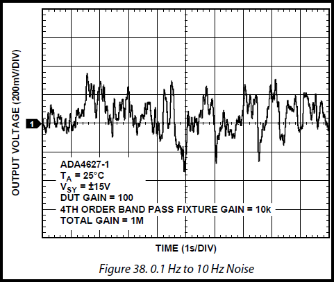
The plot is from the Analog Devices ADA4627 datasheet

Related Articles
- Basic Circuit Simulation with LTspice
- Intermediate LTspice Tutorial
- Noise Analysis Using LTspice Tutorial
- How to Perform Transient Analysis and Noise Source Simulation with LTspice
- What Is Electrical Noise and Where Does It Come From?


Thanks Stephen
Educational
Thanks Stephen. I am having some difficulties understanding:
1. How does (V(noise)@2-V(noise)@1)/10meg gives us the current noise? So, (input referred Voltage noise for HIGH input resistance - input referred Voltage noise for LOW input resistance)/resistance gives us current noise? Any reference would be much apprecated.
2. Does anything change for a TIA circuit where input is a current source (instead of a voltage source as in your example) connected at the inverting input terminal of the opamp? I am trying to find input referred current for this TIA circuit. But I am not sure if I should select the current source as the noise input or add another voltage source at the noninverting input of the opamp for noise analysis.
Thanks.