Facebook
 Google
 GitHub
 Linkedin
Singulation—Literally Cutting Edge—Is Gaining More Importance for Wafer Fabs
Singulation (wafer dicing) is critical for IC wafer manufacturing. Laser/plasma dicing is replacing mechanical methods. Lidrotec's laser-liquid technology offers virtually zero-damage cuts.
You may not know what it is, and may never have heard of it, but singulation technologies are vitally important—and becoming more so with each passing month.
Singulation is the final step in the semiconductor wafer fabrication process, where individual semiconductor chips (dies) are separated from the processed wafer. It is a critical operation because it directly affects device yield, reliability, and overall production cost. As semiconductor devices continue to shrink in size and become more complex, singulation technologies have evolved to meet demanding precision and cleanliness requirements.
Traditionally, mechanical dicing using diamond saw blades was the dominant singulation method. In this process, a high-speed rotating blade cuts along predefined scribe lines on the wafer. Mechanical dicing is cost-effective and suitable for many silicon-based devices.
However, it has limitations in cutting very thin wafers and fragile materials like gallium arsenide (GaAs) or compound semiconductors. The process can also introduce micro-cracks, particle contamination, and thermal damage, leading to reduced yield and reliability in advanced packaging applications.
Laser Dicing Gaining Popularity
To address these challenges, laser dicing technologies have become increasingly popular. In stealth laser dicing (SLD), a focused laser beam creates a modified layer beneath the wafer surface without damaging the top layer. The wafer is then cleaved along these modified regions, resulting in clean, smooth edges and minimal mechanical stress.
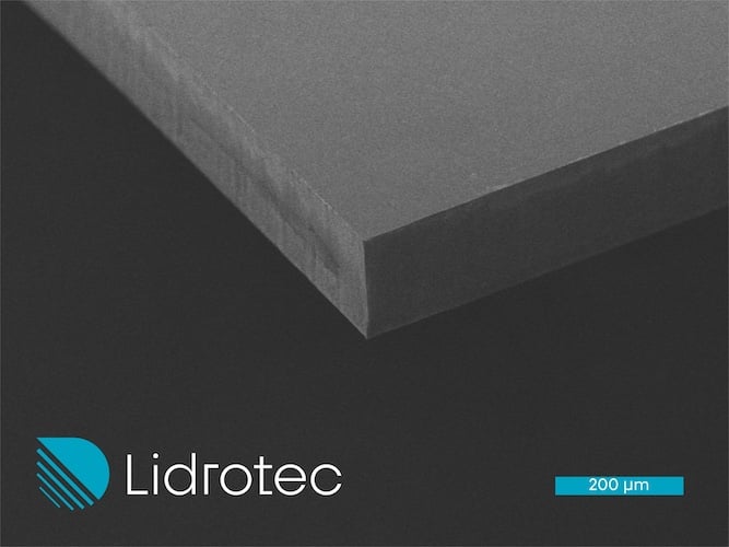
Sample cut of a 200 µm thick silicon substrate, using Lidrotec technology—with no cracks, no burr, no delamination, a very flat and clean surface.
Laser dicing offers high precision and is suitable for thin wafers used in 3D integration, MEMS, and power devices. Another variation, plasma dicing, uses reactive plasma to etch the wafer along mask-defined patterns. Plasma dicing is particularly advantageous for ultra-thin wafers and small die sizes because it eliminates mechanical contact entirely, reduces debris generation, and allows narrow kerf widths—improving chip count per wafer.
Emerging singulation techniques also include blade-laser hybrid dicing, which combines the speed of mechanical cutting with the precision of laser trimming, and water jet-guided laser dicing, which uses a water column to guide the laser beam and cool the cutting area simultaneously. These hybrid approaches aim to balance throughput, precision, and cost.
Overall, the choice of singulation technology depends on wafer material, thickness, die size, and production scale. As advanced packaging trends such as wafer-level packaging (WLP) and system-in-package (SiP) continue to grow, demand for non-contact, high-precision, and damage-free singulation methods will increase. Laser and plasma-based dicing are expected to dominate future semiconductor manufacturing due to their superior control, scalability, and compatibility with next-generation materials and device architectures.
New Singulation Technology
In order to increase yield and productivity in wafer dicing, a EU-based company called Lidrotec is bringing to market a new singulation technology. Here’s their story:
Chips are produced in a months-long process with hundreds of complicated and costly process steps until thousands, sometimes hundreds of thousands of chips are produced on a pizza-sized plate called a “wafer”. With hundreds of thousands of chips on such a wafer, each wafer is very valuable.
The last process step before the chips can be assembled into smartphones and other digital devices, is the singulation or dicing step. During this step, it is of utmost importance to cut out each chip in a way that guarantees its full functionality without any defects.
Lidrotec builds wafer dicing laser machines for the semiconductor industry that enable thinner cuts with a lower damage rate for every wafer in the singulation process. Users of this cutting-edge technology will save costs and increase output in semiconductor manufacturing.

A wafer dicing laser machine from Lidrotec
The LidroCUT technology cuts microchips more efficiently than any other laser technology. The unique innovation is the combination of a laser with a liquid flow. The liquid cools and rinses the material while it is being cut with a laser. Minimum induction of heat as well as the rinsing of debris enable microchip production with no micro cracks, no chipping and no debris on the surface.
Hence, the rate of damaged microchips during the dicing process is reduced to virtually 0%. This saves material costs and increases profitability for semiconductor manufacturers. Additionally, valuable resources that are used to build microchips, such as rare earths or gold, can be saved, helping with the conservation of resources.
The Lidrotec Team
The founding team at Lidrotec combines diverse know-how from science, engineering and finance. The three technical co-founders, Alexander Kanitz (CTO), Jan Hoppius (CDO) and Dr. Jannis Koehler (CPO) have a very diverse technical background as they have all completed different studies in their Bachelors and Masters (Physics, Mechanical Engineering, Lasers & Photonics). Together, they have a cumulative experience in laser technology of 36 years, complementing each other in every technical aspect.
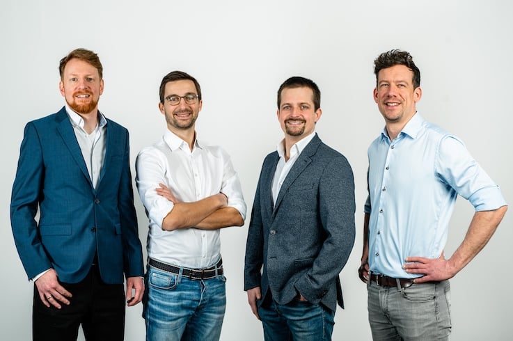
Lidrotec founders from left to right: Jannis Koehler, Alexander Igelmann, Jan Hoppius, Alexander Kanitz
In addition, the business co-founder Alexander Igelmann (CEO) adds economic and financial knowledge as well as client-facing skills to the team based on his previous work experience in the financial industry at PIMCO and Goldman Sachs.
The two Alexes, Alex K. and Alex I., have known each other for over 25 years, as they went to school together. When the three technical co-founders needed business expertise to start the company, Alex I. was the first one they contacted. In October 2019, the Lidrotec project started with a German government grant called EXIST. Since then, the company has gained traction with both investors and clients year over year.
In April 2025, Lidrotec closed a $13.5 million Series A-2 round. The round was co-led by Lam Capital, the corporate venture arm of semiconductor fabrication equipment and services company Lam Research Corporation, and Goose Capital, a venture capital firm from Houston, TX. New investors ZEISS Ventures and NRW.BANK joined the round, adding strong technical, operational and scale-up expertise.
An Increasing Need Ahead
The company expects the global semiconductor market, and with it the wafer dicing market, to continuously grow in the coming years with the main drivers being the growth of AI, the increase in electric vehicles and digitalization in general—all of which need more powerful chips. The more sophisticated, powerful and costly a chip becomes, the more yield in the dicing step matters.
All images used courtesy of Lidrotec.
Related Content